


Polycrystalline silicon has a grain oriented structure, with monocrystalline grain interior regions surrounded by grain boundaries. Polysilicon can be fabricated by a wide variety of techniques, and the physical properties and the morphological structures differ significantly.
The most common fabrication methods are:
The first method uses a CW (continuous wave) laser equipment to anneal partial implantation damage within an amorphous silicon layer. Due to the heavy ion bombardment the regularity of the silicon matrix was destroyed. The energy of the light beam melts the silicon crystal and, hence, recrystallization occurs. The grain size of the recrystallized silicon can be controlled by the laser power. CW-laser annealing is applied on a limited area, while the zone melting recrystallization is used to fabricate large-area polysilicon layers. An IR (infrared) or UV (ultra violet) source is scanned across the wafer and, thus, a narrow but large polysilicon recrystallization zone is created.
The molecular beam epitaxy (MBE) is the most expensive method. It operates at lower temperatures than the other methods, so the annoying dopant redistribution is suppressed. An evaporated molecular beam is directed towards the substrate surface. The low vapor pressure of silicon ensures the condensation of the material on the surface.
The most common method for fabrication of polysilicon layers for VLSI
circuits is pyrolizing silane ![]() between
between ![]() and
and ![]() in a low pressure ambient, which is referred to as low pressure
chemical vapor deposition (LPCVD). The chemical reaction is given by
(3.2-1).
in a low pressure ambient, which is referred to as low pressure
chemical vapor deposition (LPCVD). The chemical reaction is given by
(3.2-1).
Polysilicon LPCVD depositions are limited to the above cited temperature
range, because at higher temperatures gas phase reactions will result in
rough, loosely adhesion, and silane depletion. On the other hand, at
temperatures under ![]() , the deposition rate would be too low for
practical applications.
, the deposition rate would be too low for
practical applications.
The polysilicon deposition rate is a strong nonlinear function and depends
on the partial pressure of silane, temperature and additional process gases
as shown in Figure 3.2-1. Data are taken from [Kin83]
[Har84] [Sze88]. One major advantage of CVD methods is the simple
possibility for the introduction of dopants into the deposited
material. This process is known as in-situ technique, where dopant
gases, like phosphine ![]() , arsine
, arsine ![]() or diborane
or diborane ![]() are added
to the silane. The effects onto the deposition rates are different. Diborane
increases drastically the deposition rate because of forming
are added
to the silane. The effects onto the deposition rates are different. Diborane
increases drastically the deposition rate because of forming ![]() radicals, which catalyzes the chemical reactions and, hence, increases the
deposition rate. Phosphine and arsine are absorbed on the surface and are
therefore blocking the aggregation of silane, thus the deposition rate
decreases. Data for deposition rates including silane partial pressure
dependence and in-situ doped samples are given in Figure 3.2-1.
radicals, which catalyzes the chemical reactions and, hence, increases the
deposition rate. Phosphine and arsine are absorbed on the surface and are
therefore blocking the aggregation of silane, thus the deposition rate
decreases. Data for deposition rates including silane partial pressure
dependence and in-situ doped samples are given in Figure 3.2-1.
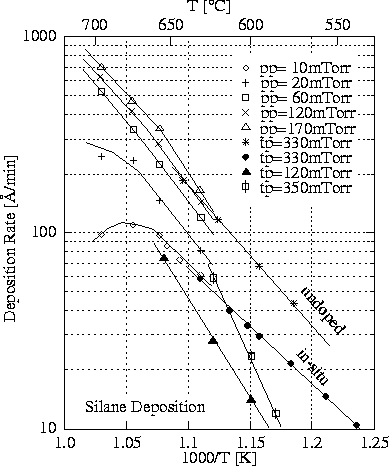
Figure 3.2-1: Deposition rates for pyrolizing of silane to fabricate polysilicon
layers. Pressure dependence (pp ![]() silane partial pressure, tp
silane partial pressure, tp ![]() silane total pressure) is also given [Kin83]
[Har84] [Sze88].
silane total pressure) is also given [Kin83]
[Har84] [Sze88].
The deposition temperature and doping conditions are affecting the
microstructure of polysilicon films drastically. Films deposited at
![]() are amorphous (see Fig. 3.2-2a), with an average
grain size below
are amorphous (see Fig. 3.2-2a), with an average
grain size below ![]() . This amorphous layer has similar properties as
silicon amorphized by ion implantation (
. This amorphous layer has similar properties as
silicon amorphized by ion implantation ( ![]() ). Ion implantation is
also a possible way to dope the polysilicon layer, but ion implantation
destroys the grain structure of polysilicon in any case. Layers deposited at
). Ion implantation is
also a possible way to dope the polysilicon layer, but ion implantation
destroys the grain structure of polysilicon in any case. Layers deposited at
![]() are only partially crystalline with a higher fraction of
amorphous islands (Fig. 3.2-2b). The grain structure and the
grain boundaries are not well defined and the average grain size is about
are only partially crystalline with a higher fraction of
amorphous islands (Fig. 3.2-2b). The grain structure and the
grain boundaries are not well defined and the average grain size is about
![]() . By adding a dopant gas the grain size is significantly
increasing (
. By adding a dopant gas the grain size is significantly
increasing ( ![]() ). Figure 3.2-2c shows the morphology of an
in-situ doped sample, where at
). Figure 3.2-2c shows the morphology of an
in-situ doped sample, where at ![]() still partially amorphous
regions exist. Therefore, a delay time must be considered before the
crystalline growth takes place [Kin83]. Polysilicon films deposited at
still partially amorphous
regions exist. Therefore, a delay time must be considered before the
crystalline growth takes place [Kin83]. Polysilicon films deposited at
![]() show columnar grains with well established grain boundaries as
given in Figure 3.2-2d. The average grain size in this case is
about
show columnar grains with well established grain boundaries as
given in Figure 3.2-2d. The average grain size in this case is
about ![]() .
.
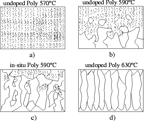
Figure 3.2-2: Microstructures of LPCVD deposited polysilicon films for different
deposition temperatures and doping conditions. Note the difference in the
amorphous portion of the layer b) undoped and c) in-situ doped. a) is
fully amorphized, where d) shows typical grain structure including grain
boundaries.
The morphological quantities of polysilicon, like average grain size
![]() , preferred grain orientation O, surface roughness
, preferred grain orientation O, surface roughness ![]() , and
the average deposition rate
, and
the average deposition rate ![]() are shown in Table 3.2-1 for a
deposition temperature range
are shown in Table 3.2-1 for a
deposition temperature range ![]() from
from ![]() up to
up to ![]() . These subtle data are necessary for an initial setup when modeling the
diffusion process. The data were obtained by X-ray diffraction measurements
[Har83] [Duf83] [Har84], where the most intense reflections
in the
. These subtle data are necessary for an initial setup when modeling the
diffusion process. The data were obtained by X-ray diffraction measurements
[Har83] [Duf83] [Har84], where the most intense reflections
in the ![]() plane are recorded.
plane are recorded.
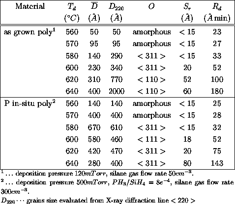
Table 3.2-1: Properties of undoped and phosphorus doped polysilicon films for
different deposition temperatures and process conditions. Data are taken
form [Har83][Duf83][Har84]. Note the
unpredictable grain size behavior of the in-situ doped sample.
If polysilicon films of high structural perfection, low strain, and small
surface roughness are required, the deposition temperature should not exceed
![]() . As a drawback it should be noted, that the deposition rate is
lower than
. As a drawback it should be noted, that the deposition rate is
lower than ![]() . Higher growth rates can be obtained at higher
deposition temperatures, but only at the cost of structural and surface
properties.
. Higher growth rates can be obtained at higher
deposition temperatures, but only at the cost of structural and surface
properties.
One of the drawbacks of polysilicon is that it changes its morphological structure at high temperatures. The grain boundaries try to migrate, and grain growth is occurring. Hence, the thorough modeling of grain growth behavior is essential for diffusion modeling within polysilicon layers.