

Next: Curriculum Vitae
Up: PhD Thesis Helmut Puchner
Previous: 6.2.3 Simulation Results
Literatur
- Ada88
-
L.M. ADAMS, R.J. LEVEQUE, AND D.M. YOUNG.
Analysis of the SOR Iteration for the 9-Point Laplacian.
SIAM J.Numer.Anal., Vol. 25, No. 5, 1988, pp. 1156-1180.
- Alv93
-
Ed. by A.R. ALVAREZ.
BiCMOS Technology and Applications, second edition.
Kluwer, 1993.
- Aro96
-
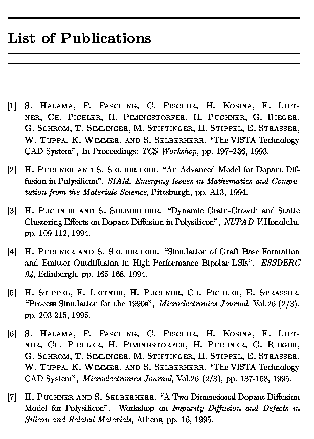
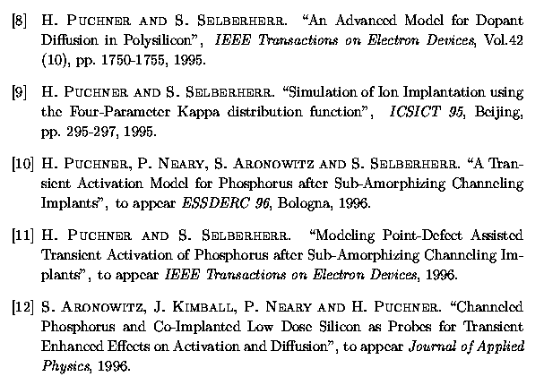
S. ARONOWITZ, J. KIMBALL, P. NEARY, AND H. PUCHNER.
Channeled Phosphorus and Co-implanted Low Dose Silicon as Probes for
Transient Enhanced Effects on Activation and Diffusion.
J.Appl.Phys., 1996.
to appear.
- Bac92
-
B. BACCUS.
A Study of Nonequilibrium Diffusion Modeling - Applications to Rapid
Thermal Annealing and Advanced Bipolar Technologies.
IEEE Trans.Electron Devices, Vol. 39, No. 3, 1992,
pp. 648-661.
- Bac95
-
B. BACCUS AND E. VANDENBOSSCHE.
Modeling High Concentration Boron Diffusion with Dynamic Clustering:
Influence of the Initial Conditions.
Microelectronics Journal, Vol. 26, 1995, pp. 235 - 242.
- Ban80
-
R.E. BANK AND D.J. ROSE.
Parameter Selection for Newton-like Methods Applicable to Nonlinear
Partial Differential Equations.
SIAM J.Numer.Anal., Vol. 17, No. 6, 1980, pp. 806-822.
- Ban81
-
R.E. BANK AND D.J. ROSE.
Global Approximate Newton Methods.
Numer.Math., Vol. 37, 1981, pp. 279-295.
- Ban94
-
R.E. BANK.
PLTMG: A Software Package for Solving Elliptic Partial
Differential Equations, Vol. 15 of Frontiers in Applied Mathematics.
SIAM, Philadelphia, 1994.
Users' Guide 7.0.
- Bor88
-
J. BORLAND, M. GANGANI, R. WISE, S. FONG, Y. OKA, AND Y. MATSUMOTO.
Silicon Epitaxial Growth for Advanced Device Structures.
Solid State Technology, 1988, pp. 111-119.
- Bro87
-
G.B. BRONNER AND J.D. PLUMMER.
Gettering of Gold in Silicon: A Tool for Understanding the Properties
of Silicon.
Appl.Phys.Lett., Vol. 61, No. 12, 1987, pp. 5286-5288.
- Chi82
-
K.Y. CHIU, J.L. MOLL, AND J. MANOLIU.
A Bird's Beak Free Local Oxidation Technology Feasible for VLSI
Circutis Fabrication.
IEEE Trans.Electron Devices, Vol. 29, No. 4, 1982,
pp. 536-540.
- Cow90a
-
N.E. COWERN, K.T. JANSSEN, AND H.F. JOS.
Transient Diffusion of Ion-Implanted B in Si: Dose, Time, and Matrix
Dependence of atomic and electrical Profiles.
J.Appl.Phys., Vol. 68, No. 12, 1990, pp. 6191-6189.
- Cow90b
-
N.E. COWERN, H.F. JOS, K.T. JANSSEN, AND A.J. WACHTERS.
Anormalous Transient Diffusion of Boron in Silicon: Kinetic Modeling
of Diffusion and Cluster Formation.
In Proceedings: Materials Research Symposion Proceedings, 1990,
Vol. 163, Materials Research Society, pp. 605-608.
- Deu74
-
P. DEUFLHARD.
A Modified Newton Method for the Solution of Ill-Conditioned Systems
of Nonlinear Equations with Application to Multiple Shooting.
Numer.Math., Vol. 22, 1974, pp. 289-315.
- Dun92
-
S.T. DUNHAM.
A Quantitative Model for the Coupled Diffusion of Phosphorus and
Point Defects in Silicon.
J. Electrochem. Soc., Vol. 139, No. 9, 1992, pp. 2628-2636.
- Duv88
-
S.G. DUVALL.
An Interchange Format for Process and Device Simulation.
IEEE Trans.Computer-Aided Design, Vol. 7, No. 7, 1988,
pp. 741-754.
- Eis81
-
S.C. EISENSTAT, M.H. SCHULTZ, AND A.H. SHERMAN.
Algorithms and Data Structures for Sparse Symmetric Gaussian
Elimination.
SIAM J.Sci.Stat.Comput., Vol. 2, No. 2, 1981, pp. 225-237.
- Ekl89
-
R. EKLUND, C. WEI, C. BLANTON, T. HOLLOWAY, M. RODDER, AND R.HAKEN.
A 0.5-
 BiCMOS Technology for Logic and 4Mbit-class SRAM's.
In Proceedings: Int.Electron Devices Meeting, 1989,
pp. 425-428.
- Fah83
-
P. FAHEY, R.W. DUTTON, AND M. MOSLEHI.
Effect of thermal nitridation processes on boron and phosphorus in
;SPMlt;100;SPMgt; silicon.
Applied Physics Letters, Vol. 43, No. 7, 1983, pp. 683-685.
- Fai77
-
R.B. FAIR AND J.C.C. TSAI.
A Quantitative Model for the Diffusion of Phosphorus in Silicon and
the Emitter Dip Effect.
J.Electrochem.Soc., Vol. 124, No. 7, 1977, pp. 1107-1117.
- Fas91
-
F. FASCHING, C. FISCHER, S. HALAMA, H. PIMINGSTORFER, H. READ, S. SELBERHERR, H. STIPPEL, W. TUPPA, P. VERHAS, AND K. WIMMER.
A New Open Technology CAD System.
In Proceedings: 21st European Solid State Device Research
Conference - ESSDERC'91, Montreux, Switzerland, 1991, Vol. 15 of
Microelectr.Eng., Ed. by M. ILEGEMS AND M. DUTOIT, Elsevier,
pp. 217-220.
- Fas94a
-
F. FASCHING.
The Viennese Integrated System for Technology CAD
Applications-Data Level Design and Implementation.
Dissertation, Technische Universität Wien, 1994.
- Fas94b
-
F. FASCHING, W. TUPPA, AND S. SELBERHERR.
VISTA-The Data Level.
IEEE Trans.Computer-Aided Design, Vol. 13, No. 1, 1994,
pp. 72-81.
- Fis94
-
C. FISCHER AND S. SELBERHERR.
Optimum Scaling of Non-Symmetric Jacobian Matrices for Threshold
Pivoting Preconditioners.
In Proceedings: Int. Workshop on Numerical Modeling of Processes
and Devices for Integrated Circuits NUPAD V, Honolulu, 1994, pp. 123-126.
- Fra83
-
A.F. FRANZ, G.A. FRANZ, S. SELBERHERR, C. RINGHOFER, AND P. MARKOWICH.
Finite Boxes - A Generalization of the Finite Difference Method
Suitable for Semiconductor Device Simulation.
IEEE Trans.Electron Devices, Vol. ED-30, No. 9, 1983,
pp. 1070-1082.
- Gil91
-
M.D. GILES.
Transient Phosphorus Diffusion Below the Amorphization Threshold.
In Proceedings: 2nd Int. Symp. Process Physics and Modeling in
Semiconductor Technology, 1991, pp. 273-286.
- Gue82
-
E. GUERRERO, H. PöTZL, R. TIELERT, M. GRASSERBAUER, AND G. STINGEDER.
Generalized Model for the Clustering of AS Dopants in Si.
J.Electrochem.Soc., Vol. 129, No. 8, 1982, pp. 1826-1831.
- Hal93
-
S. HALAMA, F. FASCHING, C. FISCHER, H. KOSINA, E. LEITNER, CH. PICHLER, H. PIMINGSTORFER, H. PUCHNER, G. RIEGER, G. SCHROM, T. SIMLINGER, M. STIFTINGER, H. STIPPEL, E. STRASSER, W. TUPPA, K. WIMMER, AND S. SELBERHERR.
The Viennese Integrated System for Technology CAD Applications.
In Proceedings: Technology CAD Systems, 1993, Ed. by F. FASCHING, S. HALAMA, AND S. SELBERHERR, Springer, pp. 197-236.
- Hal95
-
S. HALAMA, F. FASCHING, C. FISCHER, H. KOSINA, E. LEITNER, P. LINDORFER, CH. PICHLER, H. PIMINGSTORFER, H. PUCHNER, G. RIEGER, G. SCHROM, T. SIMLINGER, M. STIFTINGER, H. STIPPEL, E. STRASSER, W. TUPPA, K. WIMMER, AND S. SELBERHERR.
The Viennese Integrated System for Technology CAD Applications.
Microelectronics Journal, Vol. 26, No. 2/3, 1995, pp. 137-158.
- Hay93
-
J.D. HAYDEN, J.D. BURNETT, A.H. PERERA, T.C. MELE, F.W. WALCZYK, V. KAUSHIK, C.S. LAGE, AND Y.CH. SEE.
Integration of a Double-Polysilicon Emitter-Base Self-Aligned Bipolar
Transistor into a 0.5-
 BiCMOS Technology for Fast 4-Mb SRAM's.
IEEE Trans.Electron Devices, Vol. 40, No. 6, 1993,
pp. 1121-1128.
- Hay94
-
J.D. HAYDEN, R.C. TAFT, P. KENKARE, C. MAZURé, C. GUNDERSON, B.-Y. NGUYEN, M. WOO, C. LAGE, B.J. ROMAN, S. RADHAKRISHNA, R. SUBRAHMANYAN, A.R. SITARAM, P. PELLEY, J.H. LIN, K. KEMP, AND H. KIRSCH.
A Quadruple Well, Quadruple Polysilicon BiCMOS Process for Fast 16 Mb
SRAM's.
IEEE Trans.Electron Devices, Vol. 41, No. 12, 1994,
pp. 2318-2325.
- Hei92
-
O. HEINREICHSBERGER, M. STIFTINGER, S. SELBERHERR, AND K.P. TRAAR.
Fast Iterative Solution of Carrier Continuity Equations for
Three-Dimensional Device Simulation.
SIAM J.Sci.Stat.Comput., Vol. 13, No. 1, 1992, pp. 289-306.
- Ike87
-
T. IKEDA, A. WATANABE, J. NISHIO, I. MASUDA, N. TAMBA, M. ODAKA, AND K. OGIUE.
High-Speed BiCMOS Technology with a Buried Twin Well Structure.
IEEE Trans.Electron Devices, Vol. 34, No. 6, 1987,
pp. 1304-1310.
- Jon88
-
S.K. JONES AND C. HILL.
Modelling Dopant Diffusion in Polysilicon.
In Proceedings: Simulation of Semiconductor Devices and
Processes, Bologna, 1988, Vol. 3, Ed. by G. BACCARANI AND M. RUDAN,
Tecnoprint, pp. 441-447.
- Jop93
-
W. JOPPICH AND S. MIJALKOVIC.
Multigrid Methods for Process Simulation.
Springer, 1993.
- Kal90
-
S. KALAINATHAN, R. DHANASEKARAN, AND P. RAMASAMY.
Grain Size and Size Distribution in Heavily Phosphorus doped
Polycrystalline Silicon.
Journal of Crystal Growth, Vol. 104, 1990, pp. 250-256.
- Kan94
-
W. KANERT.
SIMS Measurements of Polysilicon Outdiffusion Experiments using
Arsenic.
SIEMENS, München, 1994.
- Kas90
-
M. KASE, M. KIMURA, H. MORI, AND T. OGAWA.
Eliminating Channeling Tail by Lower Dose Preimplantation.
Appl.Phys.Lett., Vol. 56, No. 13, 1990, pp. 1231-1232.
- Kir91
-
J. KIRCHGESSNER, J. TEPLIK, V. ILDEREM, D. MORGAN, R. PARMAR, S. WILSON, J. FREEMAN, C. TRACY, AND S. COSENTINO.
An Advanced 0.4
 BiCMOS Technology for High Performance Asic
Applications.
In Proceedings: Int.Electron Devices Meeting, 1991,
pp. 97-100.
- Kod92
-
J. KODATE, M. MIYAKE, AND S. KONAKA.
Diffusion for Uniforming Ion Implantated As Profile in Polysilicon.
Fall Meeting, The Japanese Society of Applied Physics,
Vol. 18a-ZT-1, 1992, pp. 718-719.
- Lau90
-
F. LAU.
Modelling of Polysilicon Diffusion Sources.
In Proceedings: Int.Electron Devices Meeting, 1990, Vol. 90,
pp. 737-740.
- Lau92
-
F. LAU.
Modeling of Polysilicon Diffusion Sources During Rapid Optical
Annealing.
Applied Physics A, Vol. 54, 1992, pp. 139-146.
- Mat93
-
D. MATHIOT, A. STRABONI, E. ANDRE, AND P. DEBENEST.
Boron Diffusion through thin Gate Oxides: Influence of Nitridation
and Effect on the Si/SiO
 Interface Electrical Characteristic.
J.Appl.Phys., Vol. 73, No. 12, 1993, pp. 8215-8220.
- Ogu80
-
S. OGURA, P.J. TSANG, W.W. WALKER, D.L. CRITCHLOW, AND J.F. SHEPARD.
Design and Characteristics of the Lightly Doped Drain-Source (LDD)
Insulated Gate Field-Effect Transistor.
IEEE Trans.Electron Devices, Vol. ED-27, No. 8, 1980,
pp. 1359-1367.
- Old80
-
W.G. OLDHAM, A.R. NEUREUTHER, C. SUNG, J.L. REYNOLDS, AND S.N. NANDGAONKAR.
A General Simulator for VLSI Lithography and Etching Processes:
Part II -- Application to Deposition and Etching.
IEEE Trans.Electron Devices, Vol. 27, No. 8, 1980,
pp. 717-722.
- O'N88
-
A. O'NEILL, C. HILL, J. KING, AND C. PLEASE.
A New Model for the Diffusion of Arsenic in Polycristalline Silicon.
J.Appl.Phys., Vol. 64, No. 1, 1988, pp. 167-174.
- Orl92
-
M. ORLOWSKI, H. TSENG, R. HANCE, AND P. TOBIN.
Fractal Network Diffusion of Fluorine and Boron in Polysilicon Gates.
In Proceedings: Int. Workshop on Numerical Modeling of Processes
and Devices for Integrated Circuits NUPAD IV, 1992, pp. 35-40.
- Pac95
-
P. PACKAN.
Simulating Deep Sub-Micron Technologies: An Industrial Perspective.
In Proceedings: Simulation of Semiconductor Devices and
Processes, 1995, Vol. 6, Ed. by H.RYSSEL, pp. 34-41.
- Pic90
-
P. PICHLER AND R. DüRR.
ICECREM 4.2 -- Simulation Program for Processing Steps in
Semiconductor Production.
User's Guide, Fraunhofer Arbeitsgruppe für Integrierte
Schaltungen, 1990.
- Pic93
-
CH. PICHLER AND S. SELBERHERR.
Rapid Semiconductor Process Design within the VISTA Framework:
Integration of Simulation Tools.
In Proceedings: Proceedings of the IASTED International
Conference, Pittsburgh, PA, USA, 1993, Modelling and Simulation, Ed. by M.H. HAMZA, The International Association of Science and Technology for
Development, pp. 147-150.
- Plu86
-
J.D. PLUMMER, R.W. DUTTON, J.C. BRAVMAN, B.E. DEAL, C.R. HELMS, K.C. SARASWAT, T. SIGMON, D.A. STEVENSON, W.A. TILLER, B.E. DEAL, P. FAHEY, J.P. MCVITTIE, AND S.E. HANSEN.
Process Simulators for Silicon VLSI and High Speed GaAs Devices.
Technical Report, Stanford University, 1986.
- Rie95
-
G. RIEGER, S. HALAMA, AND S. SELBERHERR.
A Programmable Tool for Interactive Wafer-State Level Data
Processing.
In Proceedings: Simulation of Semiconductor Devices and
Processes, 1995, Vol. 6, Ed. by H. RYSSEL AND P. PICHLER, Springer,
pp. 58-61.
- Rov90
-
N. ROVEDO, S. OGURA, J. ACOCELLA, K. BARNES, A. DALLY, J. BURKHARDT, T. BUTI, AND C.RICHWINE.
Process Design for Merged Complementary BiCMOS.
In Proceedings: Int.Electron Devices Meeting, 1990,
pp. 485-488.
- Saa88
-
Y. SAAD.
Preconditioning Techniques for Nonsymmetric and Indefinite Linear
Systems.
J.Comp.Appl.Math., Vol. 24, 1988, pp. 89-105.
- Saa90
-
Y. SAAD.
SPARSKIT: A Basic Tool Kit for Sparse Matrix Computations.
Technical Report, RIACS, NASA Ames Research Center, Moffett Field, CA
94035, 1990.
- Sah93
-
Z.H. SAHUL, R.W. DUTTON, AND M. NOELL.
Grid and Geometry Techniques for Multi-Layer Process Simulation.
In Proceedings: Simulation of Semiconductor Devices and
Processes, 1993, Vol. 5, Ed. by S. SELBERHERR, H. STIPPEL, AND E. STRASSER, Springer, pp. 417-420.
- Sch69
-
D.L. SCHARFETTER AND H.K. GUMMEL.
Large-Signal Analysis of a Silicon Read Diode Oscillator.
IEEE Trans.Electron Devices, Vol. ED-16, 1969, pp. 64-77.
- Sel79
-
S. SELBERHERR, W. FICHTNER, AND H. PöTZL.
MINIMOS - a Program Package to Facilitate MOS Device Design and
Analysis.
In Proceedings: Numerical Analysis of Semiconductor Devices and
Integrated Circuits, Dublin, 1979, Vol. I, Ed. by B.T. BROWNE AND J.J. MILLER, Boole Press, pp. 275-279.
- She96
-
J.R. SHEWCHUK.
Triangle: Engineering a 2D Quality Mesh Generator and Delaunay
Triangulator.
In Proceedings: First Workshop on Applied Computational
Geometry, 1996, American Computer Machinery.
- Sol90
-
S. SOLMI, E. LANDI, AND F. BARUFFALDI.
High-Concentration Boron Diffusion in Silicon: Simulation of the
Precipitation Phenomena.
J. Appl. Phys., Vol. 68, No. 7, 1990, pp. 3250-3258.
- Sol91
-
S. SOLMI, F. BARUFFALDI, AND R. CANTERI.
Diffusion of Boron in Silicon during post-implantation Annealing.
J. Appl. Phys., Vol. 69, No. 4, 1991, pp. 2135-2142.
- Spi93
-
C. SPINELLA, A. CACCIATO, F. BENYAICH, S. PANNITTERI, AND E. RIMINI.
Early Stages of the epitaxial Realignment of Poly-silicon Films onto
Silicon Substrates: Integration and Size Distribution.
In Proceedings: 1st International Rapid Thermal Processing
Conference, 1993, pp. 141-155.
- Str95
-
E. STRASSER AND S. SELBERHERR.
Algorithms and Models for Cellular Based Topography Simulation.
IEEE Trans.Computer-Aided Design, Vol. 14, No. 9, 1995,
pp. 1104-1114.
- Tan85
-
T.Y. TAN AND U. GöSELE.
Point-defects, Diffusion-Processes, and Swirl Defect Formation in
Silicon.
Applied Physics A, Vol. 37, No. 1, 1985, pp. 1-17.
- Tec94
-
TMA TSUPREME-4: Two Dimensional Process Simulation Program Version 6.1.
TECHNOLOGY MODELING ASSOCIATES.
Sunnyvale CA,USA, 1994.
- Tsa80
-
M. TSAI, F. MOREHEAD, AND J. BAGLIN.
Shallow Junctions by high-dose As Implants in Si: Experiments and
Modeling.
J.Appl.Phys., Vol. 51, No. 6, 1980, pp. 3230-3235.
- vdV92
-
H.A. VAN DER VORST.
BI-CGSTAB: A Fast and Smoothly Converging Variant of BI-CG for
the Solution of Nonsymmetric Linear Systems.
SIAM J.Sci.Stat.Comput., Vol. 13, No. 2, 1992, pp. 631-644.
- Vem81
-
V. VEMURI AND W.J. KARPLUS.
Digital Computer Treatment of Partial Differential Equations.
Prentice-Hall, 1981.
- Weh95
-
R.F. WEHOFER.
Flexibler 2-4-Baum basierter Gittergenerator für BAMBI- und
Delaunay-Gitter.
Diplomarbeit, Technische Universität Wien, 1995.
- Wil92
-
J.D. WILLIAMS.
Epitaxial Alignment of Polycrystalline Silicon and its
Implications for Analogue Bipolar Circuits.
PhD thesis, University of Southampton, United Kingdom, 1992.
- Wim90
-
K. WIMMER, R. BAUER, S. HALAMA, G. HOBLER, AND S. SELBERHERR.
Prozeß-Simulation in nichtplanaren Strukturen mit PROMIS.
In Proceedings: NuTech 90, Garmisch-Partenkirchen, 1990,
Siemens Corporate Research and Development, Germany, p. 4.
- Wim93
-
K. WIMMER.
Two-Dimensional Nonplanar Process Simulation.
Dissertation, Technische Universität Wien, 1993.
- Yos74
-
M. YOSHIDA, E. ARAI, H. NAKAMURA, AND Y. TERUNUMA.
Excess vacancy generation mechanism at phosphorus diffusion into
silicon.
J.Appl.Phys., Vol. 45, No. 4, 1974, pp. 1498-1506.


IUE WWW server
Wed Jul 10 16:10:00 MET DST 1996

