


Next: 3.2.3.3 Effective Carrier Masses
Up: 3.2.3 Band Structure Parameters
Previous: 3.2.3.1 The Band Gap
The materials given in the previous subsection are virtually
aligned to the same energy, although physically they mostly
cannot be grown on top of each other. This is done to obtain a
consistent reference energy within the simulator, which is the
midgap energy of Si, GaAs, and GaN. This alignment of the
semiconductors at the interfaces is modeled using the parameters
in Table 3.8. The alignment uses the following relations:
| |
|
 |
(3.25) |
| |
|
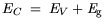 |
(3.26) |
For the transition GaN/AlN a valence band discontinuity of
 = 0.7 eV is assumed [303].
For the transition GaN/InN a valence band offset of
= 0.7 eV is assumed [303].
For the transition GaN/InN a valence band offset of  = 1.05 eV is taken.
Table 3.8:
Band gap offsets for basic semiconductors.
| Material |
 |
Material |
|
| |
[eV] |
|
[eV] |
| GaAs |
-0.712 |
GaN |
-1.715 |
| AlAs |
-1.008 |
AlN |
-2.415 |
| InAs |
-0.286 |
InN |
-0.665 |
| InP |
-0.724 |
Si |
-0.562 |
|
Next: 3.2.3.3 Effective Carrier Masses
Up: 3.2.3 Band Structure Parameters
Previous: 3.2.3.1 The Band Gap
Quay
2001-12-21