next up previous
Next: 3.2.5.2 Semiconductor Alloys Up: 3.2.5 Carrier Mobility Previous: 3.2.5 Carrier Mobility

3.2.5.1 Low Field Mobility

The first principal degradation mechanism of the low field mobility is phonon scattering in the lattice. 
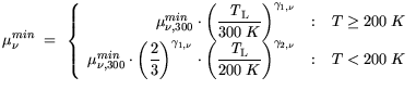
The temperature dependence is modeled according to a simple power law:

    $\displaystyle  \mu_\nu^L = \mu_{\nu 300} ^L \cdot \bigg(\frac{{\it T}_\mathrm{L}}{300 K}\bigg)^{\gamma_{0,\nu}} ,$$\displaystyle \text {where $\nu$= n,p}$ (3.35)

The corresponding material values are given in Table 3.13.


Table 3.13: Low field mobility for basic semiconductors, $ ^1$ see text for InAlAs.
Mat. $ \nu$ Valley $ \mu_n$ $ \gamma_{0,n}$ Range at low dop. References
      [cm$ ^2$/Vs] - [cm$ ^2$/Vs] (cm$ ^{-3}$ )  
GaAs n $ \Gamma$ 8500 -2.2 8100-9000 [194,273]
  p   800 -0.9 400-492 (10$ ^{15}$) [84,273,284]
  n X 410 -2.2 - [304]
AlAs n X 410 -2.1 400-1200 [273]
  p   130 -2.2 130-420 [4]
  n $ \Gamma$ 250 -2.1 - [304]
  n $ \Gamma$ 2000$ ^1$ -2.1 - [105,163]
InAs n $ \Gamma$ 32500 -1.7 22600-34000 [273,284,294]
  p   510 -2.3 200, 480, 530 [273,294]
  n X 570 -1.7 - [105]
InP n $ \Gamma$ 5300 -1.9 4200-5400 [273]
  p   200 -1.2 170, 150, 180 [273,284,294]
GaN n $ \Gamma$ 1478 -1.26 1000-1478 (MBE) [81,89,164]
        (-1.02-1.7)   [38,58]
      1700 - 1700 (MOCVD) [81]
  p   30 -1.5 - [58,259]
AlN n $ \Gamma$ 135 -1.26 - [204]
  p   14 - - [259]
InN n $ \Gamma$ 100 -1.26 100 (exp), 3200 (MC) [203,246]
  p - - - - -
Si n X 1430 -2 1500 [194,284]
  p   460 -2 450-500 [284]


Following Table 3.1 different mobilities are applied of the lowest valley at different material compositions. This allows for more precise modeling, as shown for the ternary compound semiconductors in Fig. 3.3, Fig. 3.4, and Fig. 3.5.

Figure 3.3: Comparison of the analytical models and experimental data for $ {\it N}_{\mathrm{D}}$= 5..10$ \times $10$ ^{16}$ cm$ ^{-3}$

for Al$ _{x}$Ga$ _{1-x}$As.


\includegraphics[width=10 cm]{D:/Userquay/Promotion/HtmlDiss/fig-11b.eps}

Figure 3.4: Carrier mobility as a function of material composition for In$ _x$Al$ _{1-x}$As in comparison with measurements.


\includegraphics[width=10 cm]{D:/Userquay/Promotion/HtmlDiss/fig-11.eps}

For the low field mobility of GaN a distinction is made for the growth by MBE and MOCVD, see [81]. The temperature coefficient is extracted from experimental data given by Look et al. in [164] and by MC simulations by Bhapkar et al. in [38]. For AlN the mobility is given as determined by MC simulations by Anwar et al. in [17]. For InN there is a tremendous discrepancy between various simulation predictions and the experimental values obtained. This is due to the high unintentional doping concentrations of about $ >$ 10$ ^{19}$ cm$ ^{-3}$ still prevailing in the experimental samples [246].

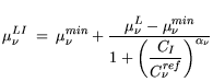
The second dominant effect degrading the transport properties is scattering due to ionized impurities (I). For binary semiconductors the following model is well established to model the dependence [62]:


    $\displaystyle \mu_\nu^{{LI}} =  \mu_{\nu}^{min} + \frac{\displaystyle \mu^L_\nu...
...^{min}}{1+ \bigg( \displaystyle \frac{C_I}{C_{\nu}^{ref}}\bigg)^{\alpha_{\nu}}}$ (3.36)
    $\displaystyle \mu_\nu^{{min}} = \left\{\begin{array}{r@{\quad:\quad}l}
\mu_{{\n...
...it T}_\mathrm{L}}{200 K}\bigg)^{\gamma_{2,\nu}} & T < 200 K
\end{array} \right.$ (3.37)
    $\displaystyle C_{\nu}^{ref} = C_{\nu,300}^{ref} \cdot \bigg( \displaystyle \frac{{\it T}_\mathrm{L}}{300 K}\bigg)^{\gamma_{3,\nu}}$ (3.38)
    $\displaystyle \alpha_\nu  = \alpha_{\nu,300} \cdot \bigg(\frac{{\it T}_\mathrm{L}}{300 K}\bigg)^{\gamma_{4,\nu}} $ (3.39)

Parameters for the influence of the impurity scattering are summarized in Table 3.14. The electron values obtained for the nitrides are taken from [89]. The saturating mobility model with no overshoot effects included is an approximation in this case for GaAs, InP, and nitride based semiconductors. For holes in GaN, the situation is rendered complicated due to compensation mechanism of the different dopands C and Mg. A compilation of experimental data is given in [98]. For InN and InGaN no experimental confirmation is available for the MC predictions so far [17,89].


Table 3.14: Model parameters for the description of the impurities.
Material Valley $ \nu$ $ \mu^{min}_{300}$ $ \gamma_{1,\nu} $ $ \gamma_{2,\nu}$ C $ ^{ref}_{\mu,300}$ $ \gamma_{3,\nu}$ $ \alpha_{nu,300}$ $ \gamma_{4,\nu}$
      [cm$ ^{2}$/Vs]     [cm$ ^{-3}$]      
GaAs $ \Gamma$ n 800 -0.9 -0.9 1.0e17 6.2 0.5 0.0
    p 40 -0.9 -0.9 1.0e17 0.5 1.0 0.0
  X n 40 -0.9 -0.9 1.0e17 0.5 0.5 0.0
AlAs X n 10 0 0 1.0e17 0 0.5 0.0
    p 5 0 0 2.9e17 0.5 1.0 0.0
  $ \Gamma$ n 10 0 0 1.0e17 0 0.5 0.0
InAs $ \Gamma$ n 11700 -0.33 -0.33 4.4e16 3.6 0.5 0.0
    p 48 0 0 2.55e17 0.5 1.0 0.0
  X n 40 -0.33 -0.33 4.4e16 0.5 0.5 0.0
InP   n 1520 2.0 2.0 6.4e16 3.7 0.5 0.0
    p 24 1.2 1.2 2.5e17 0.47 1.0 0.0
GaN   n 295 -1.02 -3.84 1e17 3.02 0.66 0.81
    p - - - - - - -
AlN   n 297 -1.82 -3.43 1e17 3.78 1.01 0.86
    p - - - - - - -
Si   n 80 -0.45 -0.15 1.12e17 3.2 0.72 0.065
    p 45 -0.45 -0.15 2.23e17 3.2 0.72 0.065


next up previous
Next: 3.2.5.2 Semiconductor Alloys Up: 3.2.5 Carrier Mobility Previous: 3.2.5 Carrier Mobility
Quay
2001-12-21