


Next: 3.3.4.2 The Ohmic Contact:
Up: 3.3.4 Semiconductor-Metal Interfaces: The
Previous: 3.3.4 Semiconductor-Metal Interfaces: The
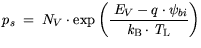
The potential at the conventional Ohmic contact interface is
calculated in a local standard model. The assumed condition for
the potential reads:
| |
|
 |
(3.99) |
with  the contact potential,
  the metal quasi Fermi-level equivalent to the applied contact voltage,
and
the metal quasi Fermi-level equivalent to the applied contact voltage,
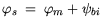
and  the built-in potential. (3.102) represents a Dirichlet condition.
The built-in potential equals the potential caused by the Fermi level adjustment
at any interface. This potential reads, as given in [90]:
the built-in potential. (3.102) represents a Dirichlet condition.
The built-in potential equals the potential caused by the Fermi level adjustment
at any interface. This potential reads, as given in [90]:
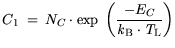
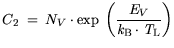
 is the overall net concentration of the applied doping at the boundary.
The auxiliary coefficients in (3.104) are defined as:
is the overall net concentration of the applied doping at the boundary.
The auxiliary coefficients in (3.104) are defined as:
| |
|
 |
(3.102) |
| |
|
 |
(3.103) |
The carrier concentrations in the semiconductor at the boundary are pinned to the
equilibrium concentrations at the contact, which read:
| |
|
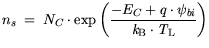 |
(3.104) |
and:
| |
|
 |
(3.105) |
This assumes a high doping of the semiconductor of the
order of
 10
10 cm
cm . Any specific interface
effects, such as dipole charges, surface charges, or a resulting
semiconductor-metal alloy, are neglected.
The carrier temperatures
. Any specific interface
effects, such as dipole charges, surface charges, or a resulting
semiconductor-metal alloy, are neglected.
The carrier temperatures
 at the Ohmic contact
are modeled as:
at the Ohmic contact
are modeled as:
| |
|
 |
(3.106) |
with
 the lattice temperature at the contact,
i.e., the carriers enter the semiconductor in thermal equilibrium.
A finite electrical line resistance of the contact metal
the lattice temperature at the contact,
i.e., the carriers enter the semiconductor in thermal equilibrium.
A finite electrical line resistance of the contact metal  can
be included using:
can
be included using:
| |
|
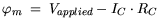 |
(3.107) |
with
 the applied terminal voltage, and
  the current through the contact.
Next: 3.3.4.2 The Ohmic Contact:
Up: 3.3.4 Semiconductor-Metal Interfaces: The
Previous: 3.3.4 Semiconductor-Metal Interfaces: The
Quay
2001-12-21