


Next: 4.7 Delay Time Extraction
Up: 4. RF-Extraction
Previous: 4.5 Interface to a
To describe limitations towards high terminal voltages the following quantities are used.
The most simple quantities are the reverse characteristics of gate diode measurements:
| |
|
 |
(4.21) |
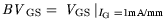
| |
|
 |
(4.22) |
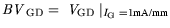
with the third terminal floating. The definition of the
voltages
 , when
 = 1 mA/mm is reached, is an
arbitrary, but generally accepted measure, since 1 mA/mm is
considered a significant damaging reverse current.
and
= 1 mA/mm is reached, is an
arbitrary, but generally accepted measure, since 1 mA/mm is
considered a significant damaging reverse current.
and
 give first indication of the breakdown hardness of the
device, especially for pseudomorphic AlGaAs/InGaAs HEMTs, where
the gate diode is limiting the maximum
give first indication of the breakdown hardness of the
device, especially for pseudomorphic AlGaAs/InGaAs HEMTs, where
the gate diode is limiting the maximum
 bias. However, as
was shown by Sommerville et al. in [270], the
extension path of the gate current
for the three terminal
device into the on-state of the transistor depends very much on
the given materials system and technology. Consequently, for
InAlAs/InGaAs values from (4.21) and (4.22) are of little practical
importance.
To evaluate a breakdown voltage for a three terminal device with the third terminal
fixed,
bias. However, as
was shown by Sommerville et al. in [270], the
extension path of the gate current
for the three terminal
device into the on-state of the transistor depends very much on
the given materials system and technology. Consequently, for
InAlAs/InGaAs values from (4.21) and (4.22) are of little practical
importance.
To evaluate a breakdown voltage for a three terminal device with the third terminal
fixed,
 is described in [270]:
| |
|
 |
(4.23) |
In this case a constant current is introduced into the gate with the source at ground,
while the drain current is swept up. Thus, the magnitude of the breakdown voltage
at
constant
is determined. This technique is useful to understand and separate the two effects,
impact ionization and thermionic field emission, as shown in Chapter 6 and 7, respectively.
Starting from a large-signal perspective, a breakdown voltage
 [76]
can be extracted from the so-called clipping behavior of a HEMT, i.e., from the generation of
nonlinearities for large voltage sweeps. Performing e.g. load-pull measurements, this results in a
breakdown locus which has an approximately quadratic behavior as a function of
, as stated
in [292].
[76]
can be extracted from the so-called clipping behavior of a HEMT, i.e., from the generation of
nonlinearities for large voltage sweeps. Performing e.g. load-pull measurements, this results in a
breakdown locus which has an approximately quadratic behavior as a function of
, as stated
in [292].
| |
|
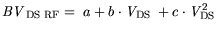 |
(4.24) |
is derived from power or load-pull contours.
The latter analysis is based on the generation of harmonics of
the operation frequency rather than on the gate-currents, although
this is related. The comparison of data obtained for  ,
,  ,
,  for the breakdown voltage is useful to determine the meaning of
the DC breakdown voltage for each device technology, since only
this behavior shows the limitations of the load matched device
for large-signal operation.
for the breakdown voltage is useful to determine the meaning of
the DC breakdown voltage for each device technology, since only
this behavior shows the limitations of the load matched device
for large-signal operation.
Next: 4.7 Delay Time Extraction
Up: 4. RF-Extraction
Previous: 4.5 Interface to a
Quay
2001-12-21