


Als einfaches Beispiel, das aber fast alle Schritte der Generierung auch komplexer Bauteile aufweist, wird die ,,Herstellung`` einer Diode gezeigt.
Die eingesetzten Einzelschritte sind Substraterzeugung, Gittergenerierung, Implantationen und Depositionen. Diese Schritte sind in eine Funktion ped::diode gepackt, die mit den gewünschten Parametern zur Steuerung der geometrischen Ausmaße und der Implantationsprofile aufgerufen wird.
Dieser Aufruf wiederum kann vom Benutzer über die Kommandozeile, über ein Kontrollfenster, von einem VLISP-Programm aus oder von außen gesteuert über den Start des PED erfolgen. Die letzte Variante ermöglicht die Verwendung in umfassenderen Abläufen wie z.B. in Optimierungsschleifen.
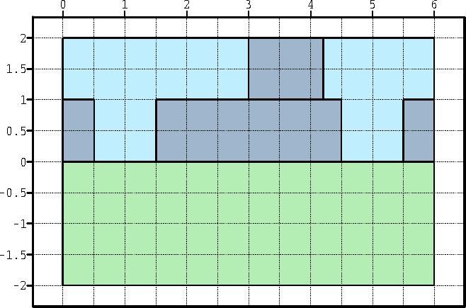
Abbildung 10.1: Die Struktur der Diode mit Kontakten
(defun ped::diode
  (width        ; the width of the diode area
   depth        ; the depth of the diode area
   hsplit       ; the horizontal grid-splitting
   vsplit       ; the vertical grid-splitting
   pwidth       ; width of Phosphorus implant
   bwidth       ; width of Boron implant
   ppeak        ; peak value of Phosphorus implant
   bpeak        ; peak value of Boron implant
   bbury        ; peak value of buried layer
   &key
   (left 0.0)                   ; left boundary of diode
   (left-contact 1.0)           ; lateral position of center of left contact hole
   (right-contact
    (- width 1.0))              ; lateral position of center of right contact hole
   (gridtype 'ORTHOGRID)        ; one of ORTHOGRID, TRI-GRID, and (not yet) LATT-GRID
   (contact-hole-width tch::CONTACT1-HOLE-WIDTH)
   (oxide1-thickness tch::OXIDE1-THICKNESS)
   (metal1-thickness tch::METAL1-THICKNESS)
   (bback 1e15)                 ; Boron background doping
   &aux x0 x1 y0 y1 s g)

  (setq x0 (float left))
  (setq x1 (+ x0 width))
  (setq y0 (- (abs depth)))
  (setq y1 0.0)

  ; make a rectangular Silicon segment
  (setq s (rectangle (list x0 y0) (list x1 y1) :material "Si"))

  ; define a grid on this segment
  (setq g (grid hsplit vsplit s :gridtype gridtype :x0 x0 :y0 y0 :x1 x1 :y1 y1))

  ; implant the dopings
  (when g
        (background-doping bback :grid g :material "B" :name "B-Implant")
        (implant (max left (+ left left-contact (- (* 0.5 pwidth))))  pwidth
                 0.0 ppeak 5 5 "P" :grid g :name "P-Implant")
        (implant (+ left right-contact (- (* 0.5 bwidth)))
                 (min bwidth (- width right-contact (- (* 0.5 bwidth))))
                 0.0 bpeak (sqrt 3.0) (sqrt 3.0) "B" :grid g)
        ; buried layer:
        (implant left width depth bbury 2 2 "B" :grid g)
        )

  ; make left oxide
  (deposit left (- left-contact (* contact-hole-width 0.5))
           oxide1-thickness  :material "SiO2")

  ; make middle oxide
  (deposit (+ left left-contact (* contact-hole-width 0.5))
           (- right-contact left-contact contact-hole-width)
           oxide1-thickness  :material "SiO2")

  ; make right oxide
  (deposit (+ left right-contact (/ contact-hole-width 2))
           (- width right-contact (/ contact-hole-width 2))
           oxide1-thickness  :material "SiO2")

  ; make left contact
  (deposit left (* 0.5 (+ left-contact right-contact))
           metal1-thickness  :depomode :flat-max  :material "Al")

  ; make right contact
  (deposit (+ left left-contact (* 0.5 contact-hole-width)
              (* 0.9 (- right-contact left-contact contact-hole-width)))
           (- width (+ left-contact (* 0.5 contact-hole-width)
              (* 0.9 (- right-contact left-contact contact-hole-width))))
           metal1-thickness  :depomode :flat-max  :material "Al")

  ; make metal1-oxide
  (deposit (+ left (* 0.5 width))
           (- (+ left-contact (* 0.5 contact-hole-width)
                 (* 0.9 (- right-contact left-contact contact-hole-width)))
              (* 0.5 width))
           metal1-thickness  :material "SiO2")
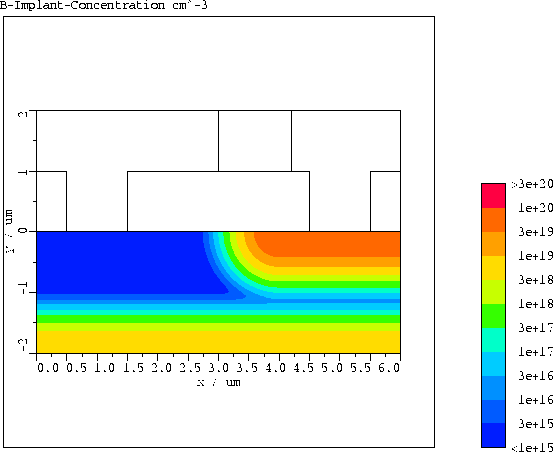
Abbildung 10.2: Die Bor-Konzentration der Diode
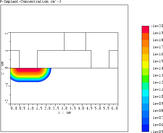
Abbildung 10.3: Die Phosphor-Konzentration der Diode