 . . |
(2.53) |
In this equation s![]() has the value -1 for n-doped material and +1 for
p-doped material, N
has the value -1 for n-doped material and +1 for
p-doped material, N![]() is the dopant concentration,
q the elementary
charge, and
VS is the surface band bending for a nonirradiated sample.
LD is the Debye length which is defined by
is the dopant concentration,
q the elementary
charge, and
VS is the surface band bending for a nonirradiated sample.
LD is the Debye length which is defined by
| LD = |
(2.54) |
For nondegenerate semiconductors the Debye length is in the order of several 10 nm.
For equilibrium and a surface states density of more than 1013 cm- 2 the position of the Fermi level in the band gap at the surface is pinned and independent from the doping concentration. This leads to band bending at the surface of the semiconductor (see Fig. 2.8).
In the surface charge analyzer method [11] this effect is used to measure the width of the potential barrier. The sample is irradiated with photons which have energies which exceed the band gap energy. The photons generate electron-hole pairs which are separated by the electric field of the potential barrier. At the surface these carriers recombine and cause a lowering of the surface potential barrier, the so called surface photo voltage VSPV. For low light intensities the surface photo voltage is proportional to the width of the barrier. The barrier width is determined by the doping concentration. For higher light intensities and especially at low temperatures the surface photo voltage saturates as the energy bands flatten [12]. The position of the Fermi level relative to the band gap at the surface is equal to that of the Fermi level in the bulk.
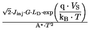
When high energy electrons are used instead of photons the situation is similar. Electron-hole pairs are generated near the surface of the semiconductor which recombine at the surface and reduce the surface potential barrier. In analogy to the surface photo voltage in the surface charge analyzer method the surface potential barrier reduction is called surface cathodo voltage VSCV [13]. The main problem in calculating VSCV and comparing it to measurements is the uncertainty in the concentration of the surface states in the band gap which strongly depends on the sample treatment.
The impact ionization generation rate G caused by the primary electrons is assumed to be independent of depth in the vicinity of the surface. For low injection rates the recombination at the surface can be described by the Schockley-Read-Hall model. For large injection rates for the current across the potential barrier at the surface the thermionic emission model is used.
A* is the effective Richardson constant which is approximately 100 A K- 2cm- 2 for electrons and 30 A K- 2cm- 2 for holes. The surface cathodo voltage can be treated as an external voltage applied to the barrier.
In steady state J is balanced by the current density JG of the carriers generated in the potential barrier.
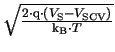
Jinj is the current density of injected primary electrons, G the generation rate, and w the barrier width which is given by
The surface cathodo voltage VSCV is determined by equating (2.55) and (2.56).
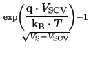 =
=  |
(2.58) |
This nonlinear equation can be solved numerically for VSCV. It should be noted that the surface cathodo voltage VSCV cannot exceed the surface band bending VS.
The energy shift ![]() E of the emitted secondary electrons is given by the
superposition of the effects due to the nonuniform doping
E of the emitted secondary electrons is given by the
superposition of the effects due to the nonuniform doping
![]() Edop and due to the surface dipole layer.
Edop and due to the surface dipole layer.
Equation (2.59) shows that for appropriately chosen primary electron energies and beam currents the energy shift of the Auger electrons is determined only by the doping.
A typical value for q . VS for n-type Si is 0.45 eV [12]. For a beam current of 100 pA and a primary electron energy of 3 keV the energy shift cause by the surface cathodo voltage is 0.489 eV.
![\resizebox{12cm}{!}{
\includegraphics[width=12cm]{eps/avcsurfaceband.eps}}](img219.gif)
 .
.