Next: 1.3.2 Solder Bumps Up: 1.3 Interconnect Technologies Previous: 1.3 Interconnect Technologies
The most innovative and efficient way in which to exploit the third dimension in wafer and die level 3D integration techniques is to employ the TSV, a direct vertical connection between different levels of a chip. It consists of a conducting via which passes through the silicon substrate and connects the two sides of the wafer. Typically, the interplane via is etched and filled with metal, such as tungsten (W) or copper (Cu) [122].
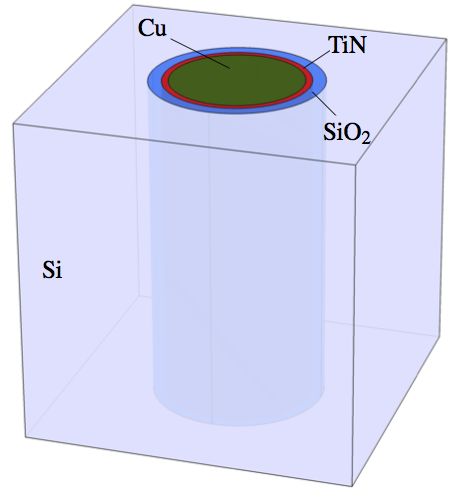
In 1.7, the general design of a TSV is shown as a cylinder of conducting material which is electrically isolated from the silicon wafer by an isolation layer, typically made of silicon dioxide (SiO2) and called TSV liner, surrounding the TSV conductor [84].
The function of the insulator is to prevent leakage and resistive coupling through the silicon [131]. Furthermore, a barrier layer, typically titanium nitride (TiN), between the liner and the conductor avoids the metal diffusion into the silicon substrate. The features of a TSV are dependent of its electrical parameters, such as metal conductivity and dielectric permittivity, and geometrical characteristics. In particular, the pitch and the aspect ratio of the TSV have a strong impact on the distribution of the TSVs during the fabrication process. TSV pitch is defined as the distance between two TSVs, while the TSV aspect ratio is determined as the ratio of the depth to the diameter of the TSV cavity. Usually, TSV structures are manufactured as an array in a silicon substrate [131]. Depending on the application and technology requirements, the maximum number of TSVs in the array is achieved only when the smallest TSV diameter with the minimum pitch is used [159]. Large size TSVs have diameters larger than 10μm, small aspect ratios of about 1 or 2, and serve as bond-pad interconnects in 3D-WLP technologies [155]. In 3D-SICs, medium size TSVs are used as global interconnects with diameters between 2μm and 10μm, while the smallest size TSVs are used at the local interconnect level.
3D integration technologies with TSVs can be realized by employing several methods, which usually involve a sequence of wafer thinning and handling, TSV formation, stacking orientation, and bonding [150]. The sequence of these basic technology modules may vary, resulting in different fabrication process flows. Diverse process approaches can be developed by changing the order of the TSV fabrication with respect to the device wafer fabrication to obtain the so-called "via first", "via middle", or "via last" process sequences. Another fabrication decision is related to the different options for stacking orientation, namely face-to-face and back-to-face alignments. Furthermore, different methods of 3D bonding, which joins two die or wafer surfaces together, depend on the key requirements of chip size, alignment accuracy, and the operations of temporary or permanent bonding [84].
A 3D system with vertical interconnects implemented as TSVs provides higher interconnect bandwidth, increased integration density, and higher performance per unit area, as well as a reduced interconnect length and power consumption when compared to the packaging level vias. Furthermore, another advantage of this approach is its resulting low contact resistance [95]. Besides its many benefits, big concerns in 3D integration with TSVs are influences of metal contamination and mechanical stress generation in the region surrounding the TSV [94]. In particular, significant thermo-mechanical stresses are induced around the TSV, when the structure is subject to temperature loading during thermal processing, due to the large mismatch in the coefficients of thermal expansion between the TSV conductor and the silicon wafer. These stresses can be high enough to influence the reliability of TSV-based 3D integration technologies. Furthermore, the TSV has limited width and thickness, due to limitations in the etching and metal deposition processes, respectively.
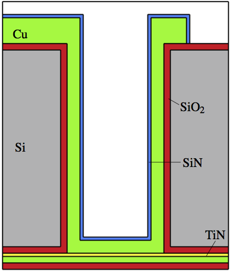
In order to overcome the thermo-mechanical issues induced by the thermal processing steps, a new concept for wafer-to-wafer integration, based on unfilled TSV technologies has been introduced in the last years [109,95,24]. The new TSV design depicted in 1.8 shows how the vertical cylinder of conducting material is replaced by a metallization layer, deposited by electroplating on the cylindrical wall of the structure, resulting in a hollow cylinder closed on the bottom side [162]. By implementing an unfilled TSV design, the so-called open TSV, the thermo-mechanical issues induced by the materials properties are minimized. Furthermore, distinctive benefits of this specific TSV technology include a relatively large TSV sidewall surface area and a thin metal layer.