Next: 5.2.3 Compact Model for Lifetime Estimation Up: 5.2 Electromigration Reliability of Solder Bumps Previous: 5.2.1 Geometry and Simulation Parameters
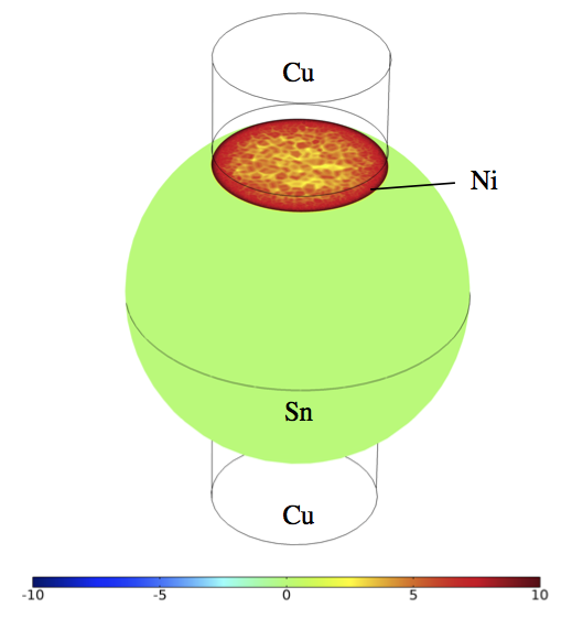
As discussed before, the nucleation of a void is related to the formation and growth of the IMC at the interface between the UBM layer and the Sn bump. Other authors have demonstrated that the growth of an IMC inside the bump under the influence of electromigration is mainly caused by the atomic fluxes of the different materials composing the geometry (JCu, JNi, and JSn), which are driven by gradients of the chemical potentials (μCu, μNi, and μSn) and the electromigration force [31,30,110,111]. The Cu and Ni atoms penetrate into the Sn bump and segregate just below the UBM/bump contact surface. The dynamics of the subsequent IMC growth is determined by the chemical reactions which convert Cu, Ni, and Sn into an IMC, typically consisting of CuSn or NiSn. The model presented in [31,30] assumes that all the transport processes take place inside the Sn bump. During the formation of the IMC, the interaction between Cu, Ni, and Sn causes hydrostatic stress because of the resulting volume change. The accumulation of atoms may give rise to compressive stresses within the solder or at the solder/UBM interface and consequent hillock formation. In turn, at the specular side of the interface, vacancy accumulation would produce tensile stress and subsequent void nucleation. The hydrostatic stress distribution in the structure is monitored as can be seen in (5.12). A tensile stress increases from the center towards the periphery of the interface between the bump and the UBM layer, which leads one to the conclusion that a void most probably nucleates at the bump/UBM interface.
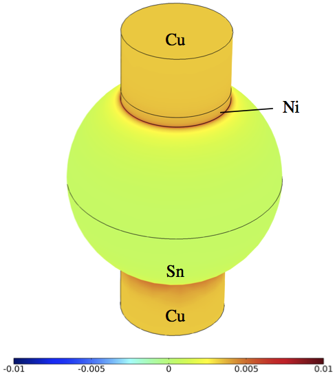
The void nucleation sites are also the locations of current crowding. This outcome can be verified by analyzing the current density distribution in the flip-chip solder bump structure, as illustrated in (5.13). Due to the different electrical conductivity of the Sn bumps and the Ni UBM layer, current crowding arises close to the interface regions of void nucleation. In fact, in the areas where the UBM layer is mechanically fixed to the Sn bump the current is mainly flowing in the bump due to its lower electrical resistance. In this way, the current flow tends to accumulate vacancies at these locations leading to a rise in tensile stresses and accordingly void nucleation [157,158].
 |