


Next: 3.2 Power Consumption
Up: 3.1 Delay Time
Previous: 3.1.5 Gate Delay
3.1.6 Clock Frequency
In a synchronous digital system (cf. Section A.3.1)
the minimum cycle time depends on the clocking scheme,
the average delay of a logic block (including storage elements),
and on the required time margin to allow for latch setup and clocking
skew. Average delay times can be used rather than maximum delays
because the gates in a critical path can usually be optimized to not
exceed this value [5].
Assuming flip-flops as storage elements and single-phase clock
3.1
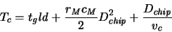
the cycle time Tc can be expressed as
 |
(3.11) |
where
 is the logic depth and
 is the chip diameter. The term
 accounts for the delays of the gates and storage elements (including
setup time and skew), and the second term represents an upper bound
for the RC-delay of global interconnections (usually on a higher
metal layer)
which cannot be reduced by inserting buffers. The last
term accounts for limitations from the speed of light or
electromagnetic waves on transmission lines. Unless very large chips
with low-resistance interconnections are considered this term is
usually negligible.
The maximum clock frequency is then the reciprocal of the cycle time:
accounts for the delays of the gates and storage elements (including
setup time and skew), and the second term represents an upper bound
for the RC-delay of global interconnections (usually on a higher
metal layer)
which cannot be reduced by inserting buffers. The last
term accounts for limitations from the speed of light or
electromagnetic waves on transmission lines. Unless very large chips
with low-resistance interconnections are considered this term is
usually negligible.
The maximum clock frequency is then the reciprocal of the cycle time:
![\begin{displaymath}
\ensuremath{f_{\mathit{c,max}}}\xspace = \left[\ensuremath{...
...p}}}\xspace }{\ensuremath{v_{\mathit{c}}}\xspace }\right]^{-1}
\end{displaymath}](img381.gif) |
(3.12) |
Footnotes
- ... clock3.1
-
(3.11) applies also to single-latch two-phase systems.
Further clocking schemes are described, e.g., in [5].
Next: 3.2 Power Consumption
Up: 3.1 Delay Time
Previous: 3.1.5 Gate Delay
G. Schrom