Reducing the gate length to the point where the depletion depth
![]() and the depletion widths of the source-bulk and drain-bulk junctions
become a significant fraction of
and the depletion widths of the source-bulk and drain-bulk junctions
become a significant fraction of
![]() leads to short-channel devices.
Although this is a purely electrical phenomenon which is independent
of geometrical scale, this transition became important as the minimum
feature size, i.e.,
leads to short-channel devices.
Although this is a purely electrical phenomenon which is independent
of geometrical scale, this transition became important as the minimum
feature size, i.e.,
![]() entered the sub-micron regime.
As a first consequence, the framework of simple drain-current
equations loses its validity. An empirical equation for
entered the sub-micron regime.
As a first consequence, the framework of simple drain-current
equations loses its validity. An empirical equation for
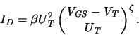
![]() is
is
![\includegraphics[scale=1.0]{real-fet.eps}](img717.gif)