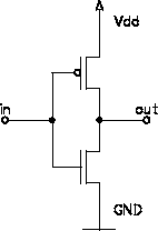
Fig. A.5 shows the circuit of a CMOS inverter,
which illustrates the principle of complementary MOS circuits: when the
input voltage is
![]() the NMOS switch is on and the PMOS is off. Thus, the
output is connected to ground only and the output voltage is 0V.
Otherwise, when the input voltage is 0V the PMOS switch is on and the
NMOS is off so that the output is connected to the supply rail.
The output of the inverter is the complement
the NMOS switch is on and the PMOS is off. Thus, the
output is connected to ground only and the output voltage is 0V.
Otherwise, when the input voltage is 0V the PMOS switch is on and the
NMOS is off so that the output is connected to the supply rail.
The output of the inverter is the complement ![]() of its input A.
Inverters are used not only for complementing a signal but also for
buffering, as line drivers and repeaters, and as amplifiers.
of its input A.
Inverters are used not only for complementing a signal but also for
buffering, as line drivers and repeaters, and as amplifiers.
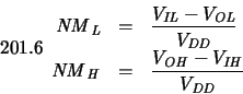
Whether an inverter works properly or not is determined by a set of
functional criteria. The first criterion is the inverter gain
![]() which
must be at least 4 (some authors require a minimum of 10).
The second criterion are the so-called noise margins
which
must be at least 4 (some authors require a minimum of 10).
The second criterion are the so-called noise margins
![]() and
and
![]() ,
i.e. the maximum noise signal which can be superimposed on a digital
signal without causing a malfunction of the circuit.
Figure A.6 shows the transfer curve of an inverter and the
definition of the noise margins.
If the output voltage of a stage plus the noise does not drive the
following stage beyond the point where
,
i.e. the maximum noise signal which can be superimposed on a digital
signal without causing a malfunction of the circuit.
Figure A.6 shows the transfer curve of an inverter and the
definition of the noise margins.
If the output voltage of a stage plus the noise does not drive the
following stage beyond the point where
![]() the noise will be attenuated rather than amplified.
Thus, the maximum/minimum input and output voltages
the noise will be attenuated rather than amplified.
Thus, the maximum/minimum input and output voltages
![]() ,
,
![]() ,
,
![]() ,
and
,
and
![]() are defined by the critical points where
are defined by the critical points where
![]() .
The noise margins are then
.
The noise margins are then
![\includegraphics[scale=0.8]{nm-def.eps}](img733.gif)