Next: 1.3.6 Temperature Behavior Up: 1.3 Characteristic Features of HCD Previous: 1.3.4 Strong Localization
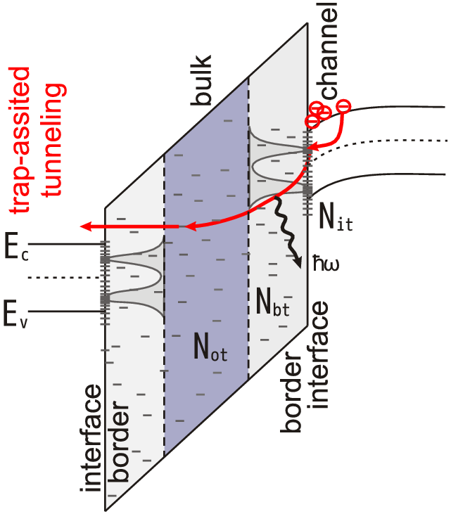
One of the essential contributions to HCD is the build-up of interface states with the corresponding concentration Nit dependent on the coordinate along the interface. These traps when charged perturb the electrostatics of the transistor (resulting e.g. in the threshold voltage shift ΔVth) and act as additional scattering centers thus degrading the mobility, transconductance and drain current. Another important component of the damage is related to the build-up of bulk oxide charge [100,101,91,66,102,103,104,60]. These traps are distributed spatially and over energy and thus have dramatically different times characterizing their charge communication (by tunneling and/or thermal activation) with Si. Depending on the length of this characteristic time, the states are conditionally separated on the border and oxide traps with densities Nbt and Not [105,106,107,41] (see Figure 1.1).
 |
In high-voltage devices the superposition of the interface states generation and oxide charge trapping accompanied by a specific field partition (compared to the conventional CMOS), Kirk effect (resulting in field redistribution) and mirror charge leads to a rather sophisticated stress behavior. For instance, the HC stress may alleviate the Kirk effect [61]. The situation is made more complicated because not only the magnitude of Nit/Not is important but its spacial location is also to be considered. Thus, if in a conventional MOSFET the degradation of Idlin is determined by the total interface state density, in the case of LDMOS the strongest impact on Idlin is contributed by states located in the drain-side spacer region [59].
While the generation of interface states during HC stress appears universally acknowledged, a considerable controversy exists regarding the build-up of bulk oxide charge. The detrimental impact of Nit on the device performance has been repeatedly reported in literature for practically every generation of CMOS devices and for various types of HC injection [2,11,12,13,14,15,16,108,109,110]. At the same time, for old CMOS technology nodes the concept that HCD is governed primarily by the interface traps localized near the drain region has been reported [5,90,89]. Therefore, for nodes smaller than 0.13um and beyond even under the worst-case conditions occurring when Vds= Vgs, the substrate current Isub is shifted from its peak, and Nit still dominates HCD [90,89]. This idea was independently confirmed by Momose et al. [111] who applied HC stresses to MOSFETs with oxide thickness varying in the range of 1.5-3.8nm where direct tunneling between the gate and channel occurs. The authors claimed that in these thin gate oxides the trapped charge immediately tunnels away and cannot be stored in the bulk of the SiO2 film. Mahapatra et al. in a series of works devoted to the determination of theNit and Not spatial distributions by means of the charge-pumping technique have suggested that in various regimes the trapped charge does not play a significant role and the degradation is dominated by Nit creation [66,102]. Finally, Polishchuk et al. investigated the reliability of MOSFET with an effective channel length of 100nm and an oxide thickness of 1.4nm. They have identified the dominant component of the degradation as Nit creation in spite the observed bulk trapping [112].
For modern ultra-scaled CMOS devices, the charge trapping in the oxide bulk becomes an issue again. Various research groups reported its presence as a drastically unfavorable factor deteriorating the performance of different types of devices with different gate oxides [113,114,115,116,117]. As for high-voltage devices, Not build-up is a commonly observed HCD component which is responsible for many peculiarities in the transformation of the transistor characteristics. [53,19,21,100,101,91,66,103,104]. The kinetics of charge trapping in the bulk of the dielectrica has been the subject of intensive research for more than four decades, i.e. starting from pioneering works by Nicollian et al. [118]. Further investigations resulted in a first-order trapping model based on the assumption that electron trapping is a stochastic process and disregarding Coulomb repulsion due to already trapped carriers and detrapping processes [119,120]. The extension of the approach in order to cover these vital features was developed by Wolters et al. [121,100] and then updated by Woltjer by linking the model to HC experimental data [101]. Therefore, the framework of this model includes injection, capture and emission. Such a sequence is typical for another intimate by related phenomenon, for trap-assisted tunneling, which is responsible for the stress-induced leakage current, a manifestation of HCD and NBTI [122,123,124,125,126,127,128,129]. For the present level of knowledge trap-assisted tunneling is an inelastic tunneling process assisted by phonon emission [130,131]. The multiphonon based models for gate oxide leakage have been proposed and verified not only for the stress-induced leakage current observed in degraded dielectric layers but also for tunnel transport through oxides and SiO2/high-k gate stacks [132,133,134,135]. This work is focused on the modeling of HCD phenomena using a reproduction of interface state density profile of a degraded device. The investigation of Nbt and Not defect contributions as well as their interplay with Nit is outside the scope of this work.