Next: 1.4.3 Reaction-Diffusion Framework Up: 1.4 Analysis and Comparison of Existing Physics-Based HCD Models Previous: 1.4.1 Hess Model
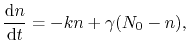
The Hess model was simplified for TCAD device simulations by Penzin [25] by employing phenomenological approximation. The model omits the microscopic level of defect generation (with the interplay of the SP- and MP-mechanisms as the essential attribute) but operates already on the device level. The bond rupture process is described by a kinetic equation for the passivated bond concentration n
where k is the forward (depassivation) reaction rate while γ is the backward (passivation) rate and N0 the total concentration of both "virgin" and broken bonds.
The forward reaction rate has the following structure:
![]() with the attempt frequency k0 and kH
being the hot-carrier acceleration factor. This term is controlled by the "local hot carrier current" [25] IHC:
with the attempt frequency k0 and kH
being the hot-carrier acceleration factor. This term is controlled by the "local hot carrier current" [25] IHC:
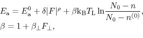
where δHC and ρHC are fitting parameters. An important peculiarity of the Penzin approach is that the activation energy of bond dissociation depends on the hydrogen density and the transversal component of the electric field. The Si/SiO2 interface (and its vicinity) is considered as a capacitor. The released hydrogen is assumed to be charged as well as the remaining dangling bonds. As a results, an additional electric field related to these charges is introduced into the system. This field prevents subsequent hydrogen ions from leaving the system and thus the potential barrier separating bonded and transport states is increased:
with E0a being the activation energy in the absence of mobile H and n(0)the preexisting mobile hydrogen concentration. Since the system is considered as a capacitor, removal of charge from the capacitor is related to an additional energy required to compensate the change of the electric field. This energy is proportional to the capacitor electric field, which is in this case the normal (to the interface) component F⊥ entering the expression. Additionally, the external electric field F can stretch or squeeze the bond, thereby changing the activation energy which is controlled by the term δ|F|ρ
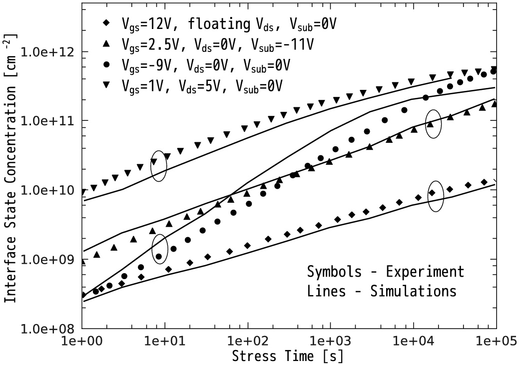
Similarly to the approach of Hess, the model employs a distribution of the activation energy and thus is able to represent the sublinear slope of degradation; Figure 1.5 demonstrates a reasonable agreement between experiment and theory. Although the model attempts to capture the carrier transport, this issue still remains vague. Formula (1.8) includes the questionable acceleration factor related to the "local hot carrier current". This criterion may be based for instance on the carrier temperature, which is related to the average energy of the distribution function (compare with the expressions (1.1) and (1.3)). As an adjacent problem, the information about the Nit profile is hardly achievable. Moreover, in spite of the efforts to link the kinetics of the trap generation and the device characteristics, one is not aware of a rigorous comparision against experimental device characteristics. Instead the soundness of the model is only proven by representing the experimental value of some cumulative Nit (Figure 1.5), but such a representation has already been obtained within the Hess approach, see Figure 1.4.
|