Next: Bibliography Up: Dissertation Ivan Starkov Previous: 5.2 Impact of Gate Oxide Thickness Variations on HCD
A comprehensive physics-based model for hot-carrier degradation must consider three different aspects: carrier transport, microscopic description of the defect build-up, and the impact of the generated defects on the device performance. While exchanging the information between these blocks one should perform a thorough check at each stage.
A direct analysis of the interface state density profile has been carried out, assessed within the developed model and that extracted from charge-pumping measurements. The approach for the modeling of the interface state density profile relies on the thorough evaluation of the carrier energy distribution function by means of a full-band Monte-Carlo device simulator. The interplay between "hot" and "colder" carriers or - in other words - the interplay between the single-particle (SP) and multiple-particle (MP) component of the Si-H bond-breakage is considered. The importance of the multiple-particle component, even in the case of long-channel devices and relatively high stress voltages, was demonstrated.
The carrier acceleration integrals for the SP and MP processes are characterized by rather different profiles. The SP-component is strongly localized near the drain end of the gate electrode while the MP-component is more or less homogeneously distributed. The latter means that under high stress conditions the MP-mechanism is still triggered. It must be linked with the low-energy part of the distribution function, which is populated under each stress conditions.
Note that in order to calculate the SP-related acceleration integral the parameter set of Bravaix et al. [30,31] is used while for the MP-component in the Keldysh-like reaction cross section the exponent of 0.1 (i.e. process is only slightly sensitive to the carrier energy variations) is used. Such a small value may be attributed to the dispersion of the parameters of the Si-H bond energetics repeatedly reported in the literature [40,24]. This question deserves more attention and has to be clarified in the future. At the moment the transport module of the approach is represented by the stochastic solver MONJU (Figure 1.12), which evaluates the carrier energy distribution function for a particular device topology. Due to a complicated transport module realization and the necessity of device conversion, additional computational noise can be seen at distribution function DF simulation. Namely, consideration of different device oxide thicknesses (real and flatted) results in a shift of the AI peak as far for electrons as for holes (see Figure 6.1). To be precise, if during simulations the oxide thickness is assumed uniform (tox(x) = tox), both AI peaks are shifted which implicitly confirms that the device architecture peculiarities must be taken into account as accurately as possible.
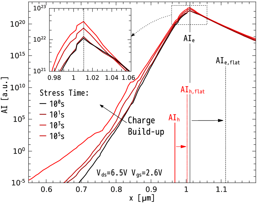 |
The thorough calculation of the DF is a time-consuming task because the key information is provided by high-energy tails of the DF which are lowly-populated. As a result, the set of distribution functions (at each position along the Si/SiO2 interface) for certain stress conditions is calculated only once and then used throughout the entire degradation time period. In reality, the DF is also distorted during the stress. For instance, the interface states - if charged - act as additional scattering centers, thereby changing the shape of the DF. Thus the DF should be recalculated at each time step. To additionally check this fact the acceleration integrals are self-consistently calculated while considering Nit(x). Figure 6.1 shows the AI vs. x and confirms the described tendency. If the position of the AI peaks does not change with time (which is in good agreement with the present model predictions where the position of the carrier acceleration integral maximum coincides with the Nit(x) peak position), the AI distribution at the middle of the channel significantly increases. However, such a consistent consideration of DF dramatically impacts the computational time and its realization within the framework with the Monte-Carlo device simulator as a transport module is practically impossible.
A potential remedy of this problem uses the flexible BTE solver ViennaSHE. In contrast to a stochastic BTE solver, which requires long computation times, a deterministic approach usually needs a high amount of memory. Certain efforts to overcome this drawback have already been performed at our Institute and realized in the device simulator ViennaSHE.
The fast BTE solver ViennaSHE will in future be used as the kernel of a comprehensive HCD model. This platform will allow for a consistent consideration of microscopic models for defect generation and carrier transport. For instance the impact of the charged traps on the carrier DF will be self-consistently incorporated. Moreover, due to the low computational costs, 3D device simulations will be possible. This is important not only for the modeling of transistors with 3D architecture but also to capture self-heating effects, which play a significant role e.g. in the context of high-voltage devices.
Another refinement is associated with the interplay between interface, border and bulk traps. The calibration of the model is expected to allow us to resolve the spatial profiles of border/bulk traps (not only vs. x but also along the coordinate inside the oxide film) as well as their energy distributions. For this purpose it is suggested to focus on HV devices where, as expected, the bulk oxide charge plays a significant role. Note that either in the case of high-voltage transistors or while interpreting results of charge-pumping measurements all types of states - i.e. interface, border and bulk - are to be considered consistently.
To conclude, the following factors must be covered for a proper modeling of hot-carrier degradation phenomena:In addition to the profiling of Nit and Not, the shape of trap density-of states should be also obtained. This information will help us resolve the question whether the SP- and MP-mechanisms really produce two types of states with different DOS. That is, the consistent consideration of SP- and MP-components or their individual treatment should be chosen.