Since the early days of the MOS transistor, its switching capability has been exploited by a wide variety of applications. By applying a high or low voltage on the gate contact, the current flow between source and drain can be switched on or off, respectively. The off-state current was supposed to be very small, in fact, early analytical models for the electrical behavior of MOS transistors like the low-level SPICE models were even assuming a zero off-state current [37]. Commonly used equations for deriving the drain current were based on the well-known quadratic transfer curve of a MOS transistor. Below a certain gate-source voltage, called ``threshold voltage'', the drain current was supposed to be zero.
Surely, this has been a good approximation for quite some time when long channels and high supply voltages were used. Then the semiconductor industry started shrinking the devices to increase their density on a chip leading to a higher power dissipation since the active chip area stayed the same or was even increased to benefit from a higher system complexity. Additionally, the electric fields in the device were constantly increasing because the voltage drops over the gate oxide and the channel stayed the same while their sizes were reduced, leading to reliability concerns.
Consequently, the supply voltage was decreased to overcome these problems though the scaling method applied to the supply voltage has been much more conservative than the one for the device geometry [7,62]. The threshold voltage was decreased, accordingly, to maintain good driving capabilities.
As a result, the off-state current gradually became a limiting factor for down-scaling the threshold voltage since it determines the power consumption of a chip in its idle state. It could not be ignored longer and new physical models had to be applied to correctly describe the device behavior in the so-called subthreshold or weak-inversion regime [13,17,28].
Basically, three different regimes can be defined for the operation of a MOS transistor. Based on the inversion condition of the channel, these regimes are called weak inversion, moderate inversion, and strong inversion. In general, two mechanisms are responsible for the current flow: drift and diffusion.
Under weak inversion the channel surface potential is almost constant across the channel and the current flow is determined by diffusion of minority carriers due to a lateral concentration gradient. Under strong inversion there exists a thin layer of minority carriers at the channel surface and a lateral electric field which causes a drift current. The moderate inversion regime is considered a transition region between weak and strong inversion where both current flow mechanisms coincidently exist [65].
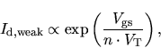
In the weak-inversion (or subthreshold) regime, the drain current depends
exponentially on the gate-source voltage [65]
 |
(2.2) |
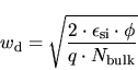
The subthreshold slolpe factor ![]() of a long-channel uniformly doped device
can be calculated using simple expressions for the gate and bulk capacitances
of a long-channel uniformly doped device
can be calculated using simple expressions for the gate and bulk capacitances
![]() and
and ![]() ,
respectively
,
respectively
The exponential subthreshold behavior can be explained by the exponential
dependence of the minority carrier density on the surface potential which,
itself, is proportional to the gate voltage. On a semi-logarithmic scale the
transfer (or
![]() -
-
![]() )
curve in the subthreshold regime will, therefore, be
a straight line.
)
curve in the subthreshold regime will, therefore, be
a straight line.
The slope of this line is called ``subthreshold slope''. The inverse of this
slope is usually referred to as ``subthreshold swing'' ![]() ,
given in units
(mV/decade) and can be derived from (2.1)
,
given in units
(mV/decade) and can be derived from (2.1)
Due to the bulk effect the subthreshold swing of a conventional MOS transistor
in bulk technology will always be higher than a certain optimum value which is
roughly 60 mV/dec at room temperature, and which can be calculated by setting
![]() equal to 1 in (2.6) which means that the bulk effect is fully
suppressed
equal to 1 in (2.6) which means that the bulk effect is fully
suppressed
A small subthreshold swing is highly desired since it improves the ratio
between the on- and off-currents. This requires that the bulk charge in the
depletion region under the channel changes as little as possible when the gate
voltage varies, therefore ![]() should be small. Any additional bulk
charge increases the voltage drop between the channel surface and the bulk
contact, thus reducing the impact of the gate voltage on the surface
potential.
should be small. Any additional bulk
charge increases the voltage drop between the channel surface and the bulk
contact, thus reducing the impact of the gate voltage on the surface
potential.
A small ![]() can be established by a light bulk doping
can be established by a light bulk doping
![]() under the channel since the depletion width in (2.4) is
proportional to the inverse square root of the doping level:
under the channel since the depletion width in (2.4) is
proportional to the inverse square root of the doping level:
Fig. 2.1 shows a couple of transfer curves of a quarter-micron MOS transistor for different bulk doping levels. There exists a doping for which the subthreshold swing has an optimum. For higher doping levels the bulk effect becomes stronger like described above.
![\resizebox{0.95\textwidth }{!}{
\psfrag{xlabel} [ct][ct] {gate voltage {
{$V_{\m...
... {1.5}
\includegraphics[width=0.95\textwidth ]{../figures/phenomena-curves.eps}}](img43.gif)
|
For very low doping levels this behavior is reversed, caused by an effect
similar to the punchthrough effect [74] explained in
Section 2.2. To demonstrate this, two devices with different bulk
doping levels are investigated in the weak inversion regime under a constant
drain current condition of 46 pA. Device ![]() has a bulk doping of
3.16
has a bulk doping of
3.16![]() 10
10![]() cm
cm![]() ,
Device
,
Device ![]() has a bulk doping of
10
has a bulk doping of
10![]() cm
cm![]() .
Their operating points are indicated in
Fig. 2.1.
.
Their operating points are indicated in
Fig. 2.1.
Fig. 2.2 shows the two-dimensional potential distribution of the two
devices. It can be seen that for Device ![]() the drain and source
depletion regions reach closer together due to the decreased doping level, and
almost merge beneath the channel region.
the drain and source
depletion regions reach closer together due to the decreased doping level, and
almost merge beneath the channel region.
Therefore, the actual current path between drain and source penetrates deeper
into the bulk, as depicted in Fig. 2.3 which shows the
two-dimensional current density for Device ![]() .
Fig. 2.4
compares the electron concentrations of the two devices across a vertical
cut-line in the channel middle. Device
.
Fig. 2.4
compares the electron concentrations of the two devices across a vertical
cut-line in the channel middle. Device ![]() has the maximum electron
concentration at the surface whereas for Device
has the maximum electron
concentration at the surface whereas for Device ![]() the maximum is
clearly under the surface. As already mentioned above, both devices deliver
the same drain current.
the maximum is
clearly under the surface. As already mentioned above, both devices deliver
the same drain current.
As a result of the increased distance of the current path to the surface, the gate contact loses more and more control over the channel which can be accounted for by a virtual increase of the gate oxide thickness and, therefore, a smaller gate capacitance according to (2.5).
For MOS transistors built in Silicon-On-Insulator (SOI) technology the subthreshold swing is usually better than in bulk technology. In fact the subthreshold swing of SOI devices can even reach the optimum value given in (2.7) depending on whether their bulk is fully depleted or partially depleted [14]. This makes SOI a promising candidate for ultra low-power CMOS applications though a lot of improvements to current process technologies still have to be made until this new technique can be applied to commercial products on a large scale [15].


![\resizebox{\textwidth}{!}{
\psfrag{x [um]}[ct][cb]{$x$\ ($\mu$m)}
\psfrag{y [um]...
...degraphics[height=\textwidth,angle=90]{../figures/phenomena-potential.16.5.eps}}](img48.gif)
![\resizebox{\textwidth}{!}{
\psfrag{x [um]}[ct][cb]{$x$\ ($\mu$m)}
\psfrag{y [um]...
...ludegraphics[height=\textwidth,angle=90]{../figures/phenomena-potential.17.eps}}](img49.gif)
![\resizebox{\textwidth}{!}{
\psfrag{x [um]} [ct][cb]{$x$\ ($\mu$m)}
\psfrag{y [um...
...udegraphics[height=\textwidth,angle=90]{../figures/phenomena-currdens.16.5.eps}}](img50.gif)
![\resizebox{0.95\textwidth }{!}{
\psfrag{xlabel} [ct][ct] {vertical position y ($...
...}
\includegraphics[width=0.95\textwidth ]{../figures/phenomena-currentpath.eps}}](img51.gif)