|
|
|
|
Previous: 6.1 Bandstructure Calculations Up: 6.1 Bandstructure Calculations Next: 6.1.2 Strain-Induced Change of the Shape of the |
In Figure 6.1 the calculated band edge energies of biaxially strained Si
and Ge are compared to those of Rieger and Vogl [Rieger93]. Good
agreement can be observed for both strained Si for (001)-oriented
Si![]() Ge
Ge![]() buffers and strained Ge for (001)-oriented
Si
buffers and strained Ge for (001)-oriented
Si![]() Ge
Ge![]() buffers for the whole range of substrate mole-fractions
buffers for the whole range of substrate mole-fractions
![]() .
.
[a]![\includegraphics[width=8.cm]{xcrv-scipts/epmSubOr110_bw.eps}](img1043.png) [b]
[b]![\includegraphics[width=8.cm]{xcrv-scipts/epmSubOr111_bw.eps}](img1044.png)
|
In Figure 6.2 the band edge energies of the conduction band valleys of Si grown on
Si![]() Ge
Ge![]() buffers with orientation (110) and (111) are
presented. For (111)-oriented buffers the
buffers with orientation (110) and (111) are
presented. For (111)-oriented buffers the ![]() -valleys do not split in
agreement to the theoretical model (3.47). For (110)-oriented
buffer the splitting between the
-valleys do not split in
agreement to the theoretical model (3.47). For (110)-oriented
buffer the splitting between the ![]() -valleys of strained Si is very
small. From a deformation potential theory which neglects the lifting of the
degeneracy of the two lowest conduction bands at the
-valleys of strained Si is very
small. From a deformation potential theory which neglects the lifting of the
degeneracy of the two lowest conduction bands at the ![]() points the splitting
cannot be reproduced. Using the deformation potential theory the valley shift
between the
points the splitting
cannot be reproduced. Using the deformation potential theory the valley shift
between the
![]() -valley pair and the
-valley pair and the
![]() -valley pair
increases linearly with strain [Singh93]
-valley pair
increases linearly with strain [Singh93]
| (6.1) |
When taking into account the additional valley shift of the
![]() -valley due to shear strain, the total valley shift is obtained from
-valley due to shear strain, the total valley shift is obtained from
Figure 6.3 shows that the model (6.2) agrees much better with the results of EPM calculations.
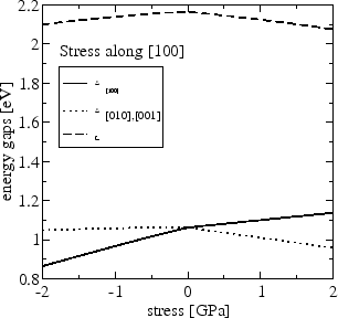
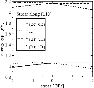
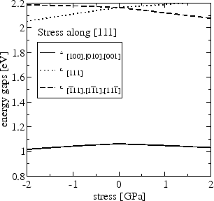
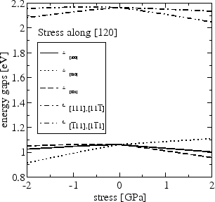
The shifts of the band edge of the ![]() -valleys and the
-valleys and the ![]() -valleys are
calculated for uniaxial stress along four different
directions. Figure 6.4 shows that the valley shifts are
linear for stress up to 2 GPa, and that the largest splitting among the
-valleys are
calculated for uniaxial stress along four different
directions. Figure 6.4 shows that the valley shifts are
linear for stress up to 2 GPa, and that the largest splitting among the
![]() -valleys is obtained for the stress direction
-valleys is obtained for the stress direction
![]() .
Since the conduction band edges are given with respect to edge of the top
valence band, which is either the heavy-hole or the light-hole band depending
on the sign of stress, the slope of the valley splitting at
0 GPa changes.
.
Since the conduction band edges are given with respect to edge of the top
valence band, which is either the heavy-hole or the light-hole band depending
on the sign of stress, the slope of the valley splitting at
0 GPa changes.
|
|
|
|
|
Previous: 6.1 Bandstructure Calculations Up: 6.1 Bandstructure Calculations Next: 6.1.2 Strain-Induced Change of the Shape of the |
![$\displaystyle \delta E_0^{\Delta_{[001]}} + \delta E_1^{\Delta_{[001]}} - \delt...
...math{\varepsilon_{\vert\vert}}} \tilde{c} \frac{\Delta}{4} \kappa^2 \right )\ .$](img1049.png)
![\includegraphics[width=11.cm]{xcrv-scipts/DeltaValleySplitEpi110_bw.eps}](img1050.png)