4.3.10 Examples
This section depicts several examples to show the usability of the introduced device simulator
approach. The examples are chosen to depict the multi-dimensional support as well as the
device template mechanism, the different simulation problems, and the stepping facility.
Implementation details as well as simulation results are shown.
One-Dimensional Capacitor
This section discusses a one-dimensional capacitor device, solving the Laplace problem
(Section 4.3.6). This particular case has been chosen to depict the support for
one-dimensional devices, usually required for developing and debugging more advanced
models. Therefore, this rather trivial device is required to be supported by every device
simulator, before delving into more complicated models.
The device consists of five segments; two metal contact segments are attached to
either side of a silicon dioxide-silicon-silicon dioxide (SiO -Si-SiO
 ) structure,
both assigned as Dirichlet contacts. As the implementation of the Laplace
problem
keeps the permittivity on the left side of the equation (Section 4.3.6), the potential
reflects the transition between the materials, as shown in Figure 4.16. The potential
drops more significantly in the oxide segments than in the middle semiconductor
segment.
) structure,
both assigned as Dirichlet contacts. As the implementation of the Laplace
problem
keeps the permittivity on the left side of the equation (Section 4.3.6), the potential
reflects the transition between the materials, as shown in Figure 4.16. The potential
drops more significantly in the oxide segments than in the middle semiconductor
segment.
Two-Dimensional PN Diode
This section shows the simulation of a two-dimensional pn-junction diode. The DD problem
(Section 4.3.6) is solved for a set of contact potentials. This particular example has been
chosen to depict the support for two-dimensional devices as well as the evaluation of device
characteristics.
The device consists of four segments, where two metal contact segments are attached to
either side of a p-Si-n-Si structure (Figure 4.17). The p-Si offers a constant donor and
acceptor doping of  cm
cm and
and  cm
cm , respectively. The n-Si offers a constant donor
and acceptor doping of
, respectively. The n-Si offers a constant donor
and acceptor doping of  cm
cm and
and  cm
cm , respectively.
The device characteristics is computed by applying a constant cathode contact potential
by simultaneously varying the anode contact potential, ranging from  V to
V to  V, with a
stepsize of
V, with a
stepsize of  V (Figure 4.18). In forward and reverse operation a maximum current of
 A and
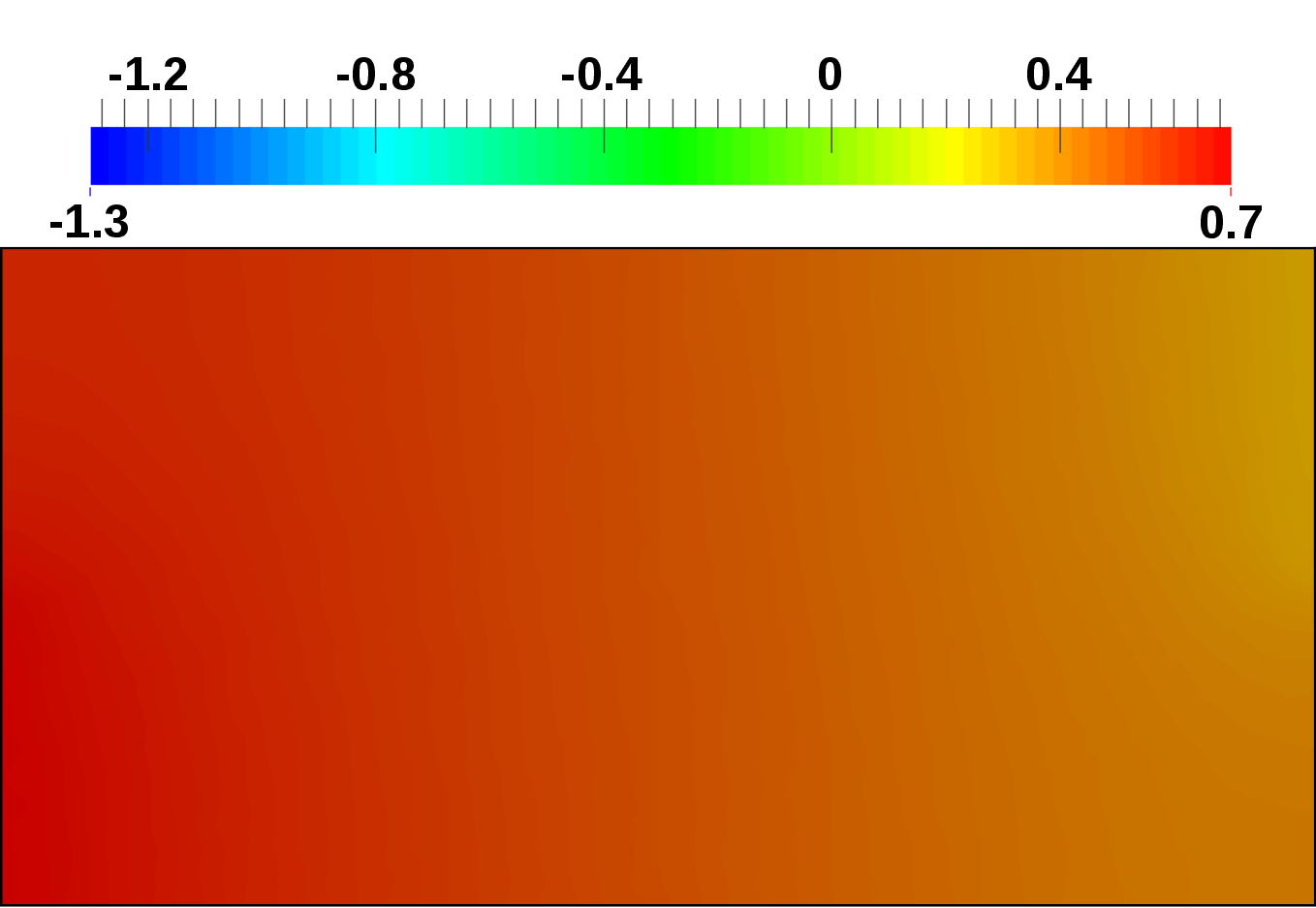
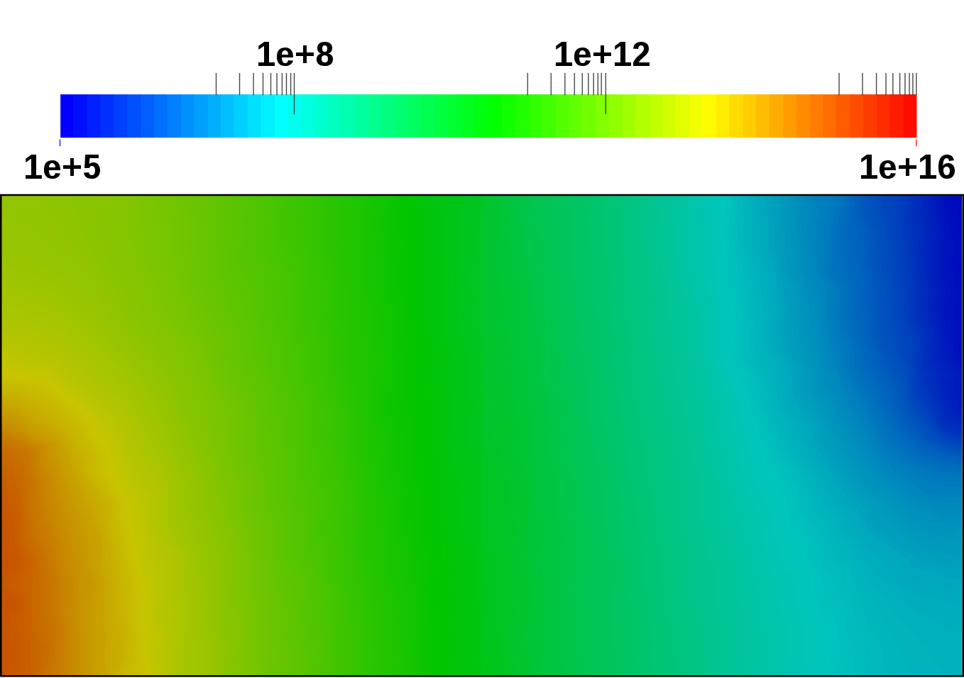
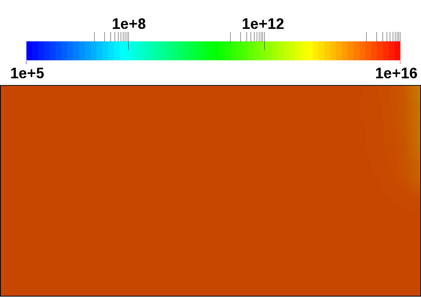
A and  nA is computed, respectively. Figure 4.19 depicts the computed potential
distributions for the reverse, equilibrium, and forward case. In the forward case, the polarity of
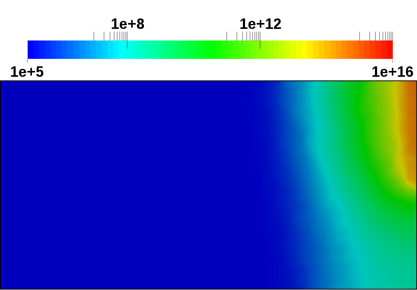
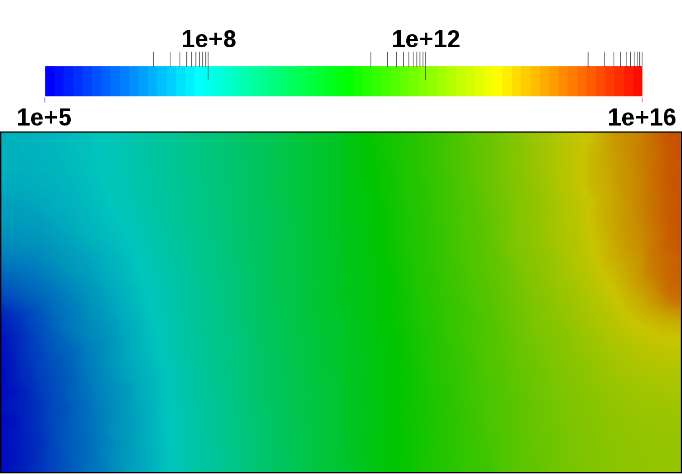
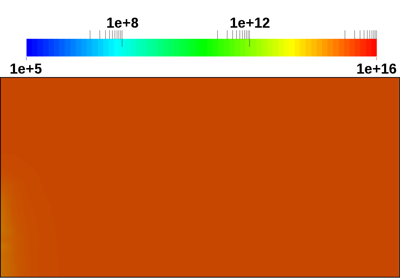
the anode contact is switched. Figure 4.20 depicts the computed electron concentration
distributions for the reverse, equilibrium, and forward case. Where in the reverse case, the
electrons retract toward the cathode contact, in the forward case the electrons are distributed
over the entire device. Figure 4.21 depicts the computed hole concentration distributions for
the reverse, equilibrium, and forward case. Where in the reverse case, the holes retract
toward the anode contact, in the forward case the holes are distributed over the entire
device.
nA is computed, respectively. Figure 4.19 depicts the computed potential
distributions for the reverse, equilibrium, and forward case. In the forward case, the polarity of
the anode contact is switched. Figure 4.20 depicts the computed electron concentration
distributions for the reverse, equilibrium, and forward case. Where in the reverse case, the
electrons retract toward the cathode contact, in the forward case the electrons are distributed
over the entire device. Figure 4.21 depicts the computed hole concentration distributions for
the reverse, equilibrium, and forward case. Where in the reverse case, the holes retract
toward the anode contact, in the forward case the holes are distributed over the entire
device.
Three-Dimensional FinFET
This section shows the simulation of a three-dimensional symmetrically sliced Si-based
FinFET device, based on solving the DD problem (Section 4.3.6). This particular example has
been chosen to depict the support for three-dimensional devices.
Figure 4.22 depicts the device setup. The source and drain region are set at a constant
donor doping of  cm
cm , whereas the bulk region is set at a constant acceptor doping of
 cm
cm .
.
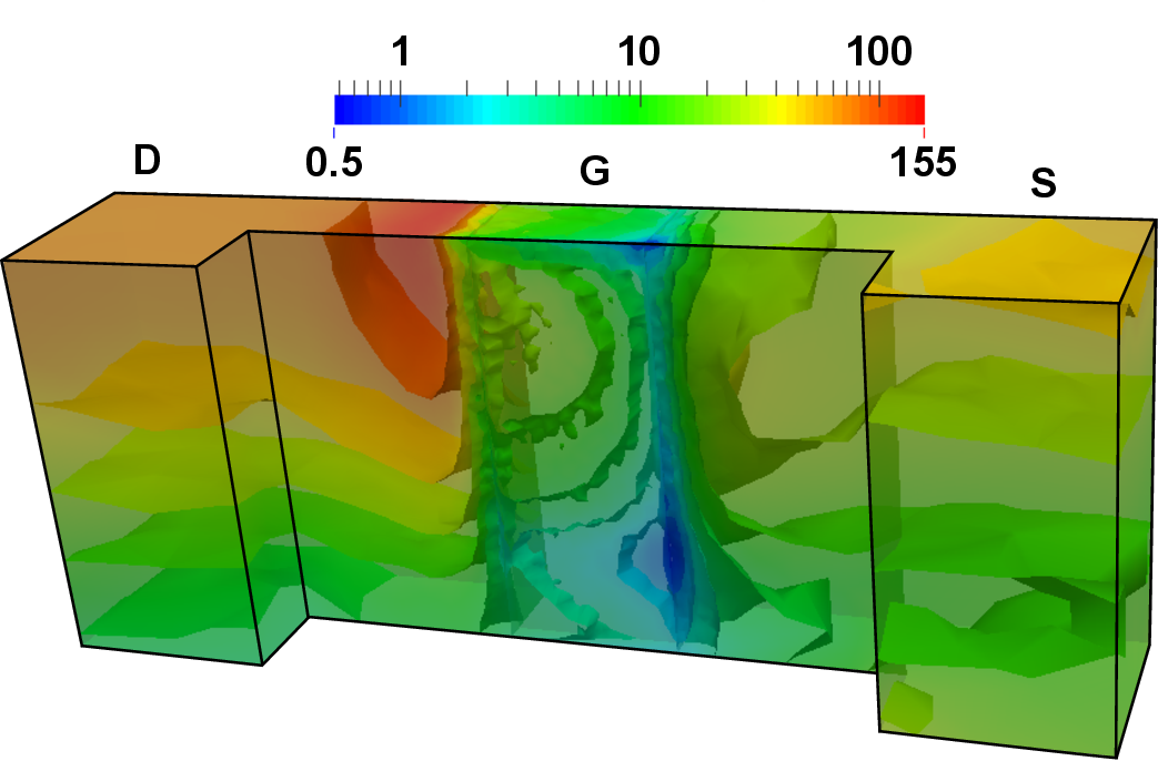
The device has been simulated in its active state, by setting the gate and drain contact
potential to  V as well as the source and bulk contact potential to
  V (Figure 4.23). As
can be seen from the results, the electrons gather primarily under the gate contact, forming a
conducting channel from the source to the drain contact.
V (Figure 4.23). As
can be seen from the results, the electrons gather primarily under the gate contact, forming a
conducting channel from the source to the drain contact.
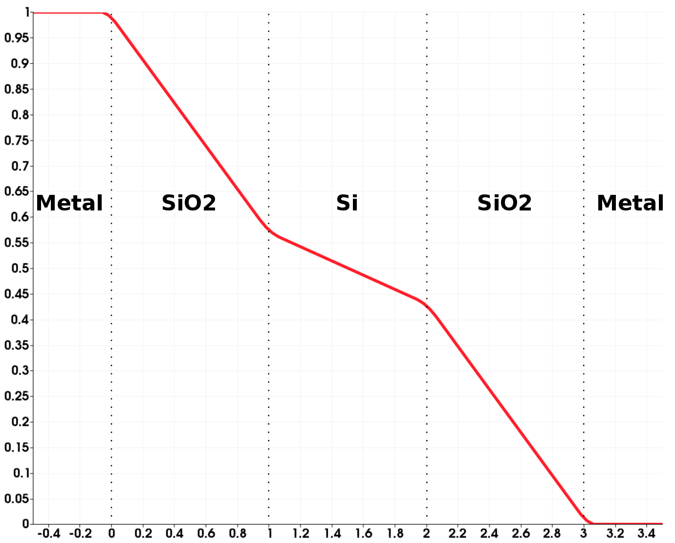
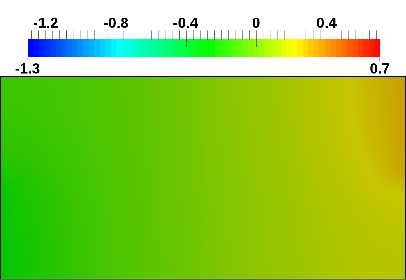
 ) of a one-dimensional
capacitor is depicted. Dirichlet boundary conditions have been applied to the left
(
) of a one-dimensional
capacitor is depicted. Dirichlet boundary conditions have been applied to the left
( V) and the right (
 V) metal contact. Note the potential transitions at the material
interfaces due to the different relative permittivities of SiO
V) metal contact. Note the potential transitions at the material
interfaces due to the different relative permittivities of SiO and Si.
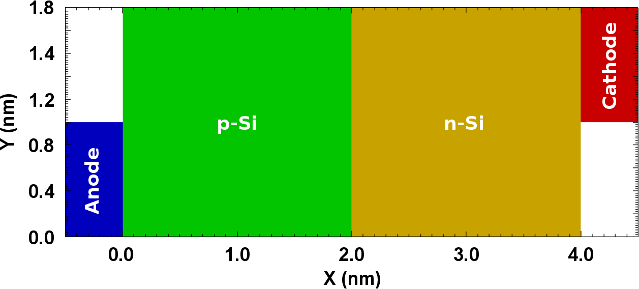
 cm
cm , respectively.
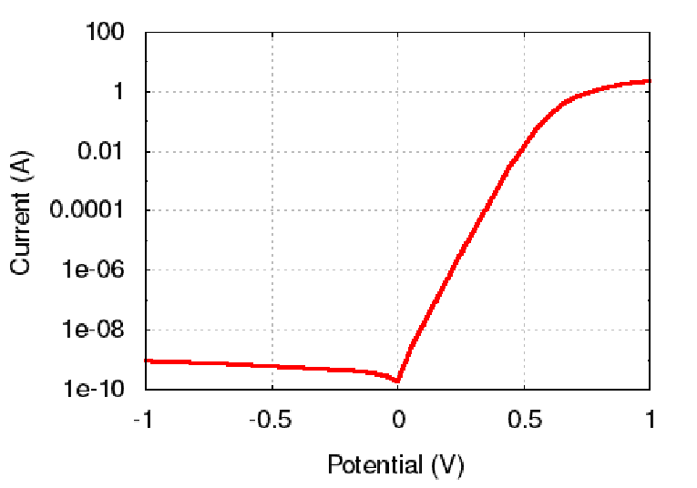
 V). For forward bias (positive
potential values) the diode is conductive, whereas for negative bias (negative potential
values) the diode is non-conductive. Note the current saturation (
V). For forward bias (positive
potential values) the diode is conductive, whereas for negative bias (negative potential
values) the diode is non-conductive. Note the current saturation ( V) induced by
high injection effects.
V) induced by
high injection effects. 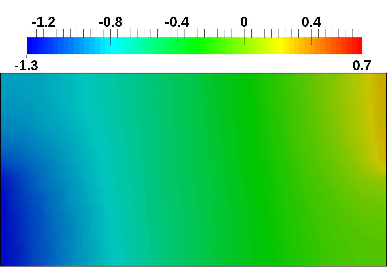
 ) in reverse (
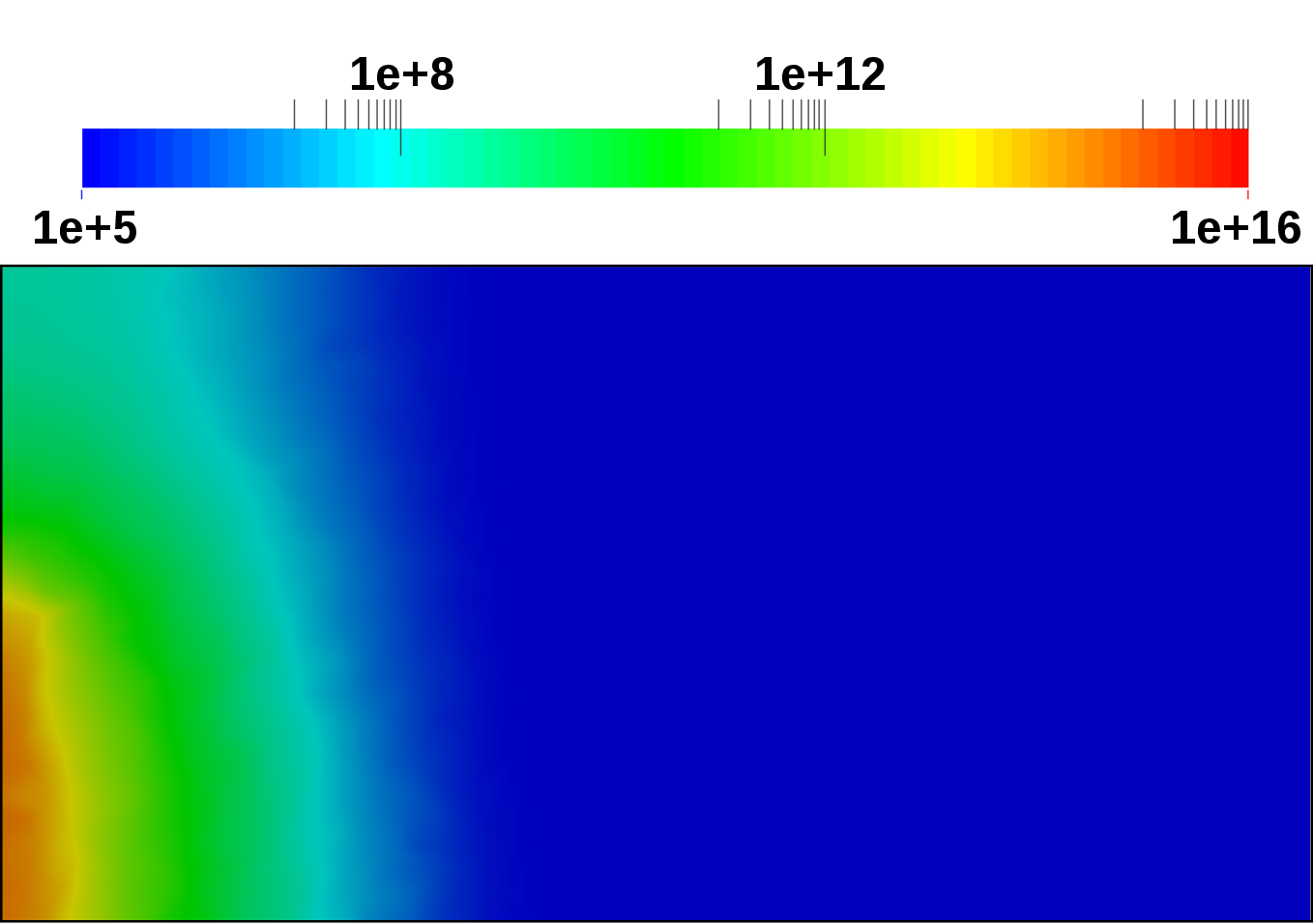
 ) in reverse (
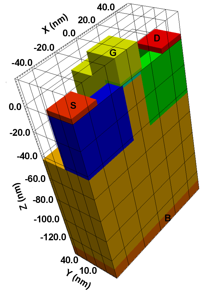
 cm
cm . The bulk (brown) region offers a constant acceptor doping of
  cm
cm .
.
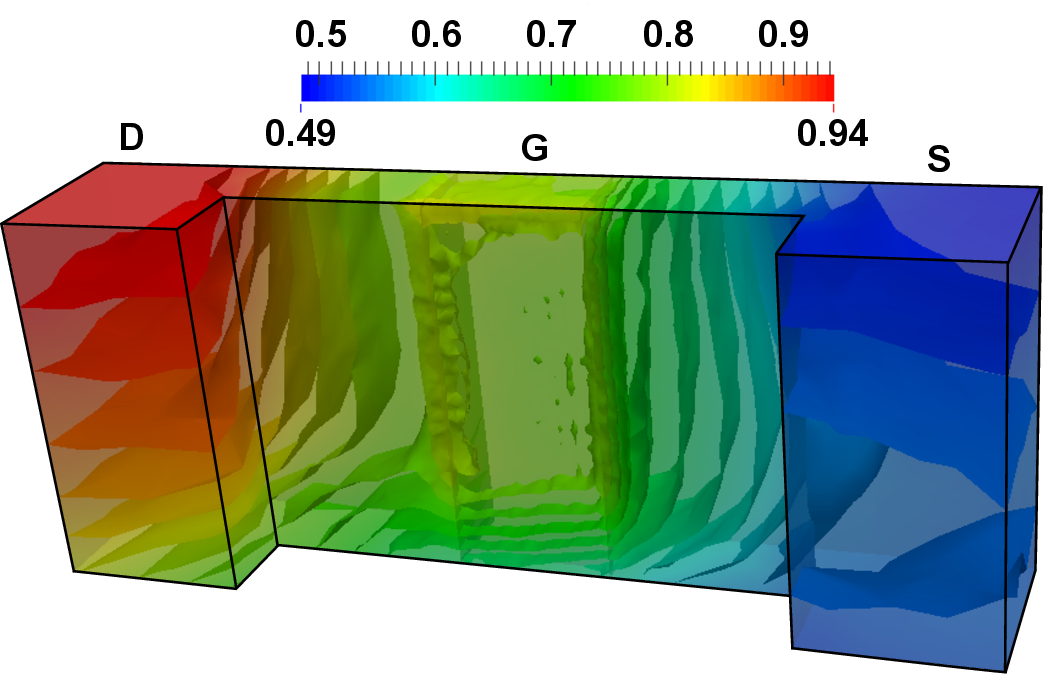
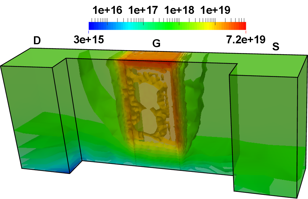


 V, whereas the source and bulk contact
potential is set to
V, whereas the source and bulk contact
potential is set to  V. The contact, oxide, and bulk segments have been removed for
the sake of improved visualization. Iso-surfaces have been added to depict the behavior
in the interior of the device. A conducting channel is formed under the gate as can be
seen from the increased electron concentrations.
V. The contact, oxide, and bulk segments have been removed for
the sake of improved visualization. Iso-surfaces have been added to depict the behavior
in the interior of the device. A conducting channel is formed under the gate as can be
seen from the increased electron concentrations.