


Next: Bibliography
Up: Appendix
Previous: D. Relation Between Charge
E. Flatband Potential and MOSFET Properties
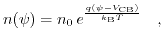
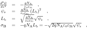
Applying a potential between drain and source leads to a charge transport and the thermal equilibrium distribution under the assumption of Boltzmann statistics is not applicable anymore. One can evade this hitch by assuming stationary conditions, meaning there is no change in charge density over time, so the carrier density can be reformulated to:
 |
(7.40) |
where
 denotes the potential value at a location C in the channel.
A procedure analogous to the one in Appendix D. yields the following expression for the total semiconductor charge:
denotes the potential value at a location C in the channel.
A procedure analogous to the one in Appendix D. yields the following expression for the total semiconductor charge:
 |
(7.41) |
This shows that the charge density depends on the value of
within the channel. In order to calculate the current in the channel, one has to define the channel width  and the channel length
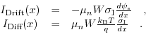
  . The current consists of a drift and a diffusive component:
 |
(7.42) |
 is the channel mobility, while
 describes the inversion charge density.
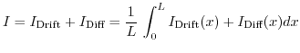
The total current is given by the sum of the diffusive and drift part and can be calculated by averaging all infinitesemal contributions along the channel.
describes the inversion charge density.
The total current is given by the sum of the diffusive and drift part and can be calculated by averaging all infinitesemal contributions along the channel.
 |
(7.43) |
Unfortunately, the inversion charge density
and the semiconductor surface potential
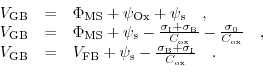
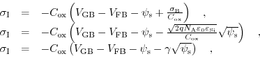
 are not easyly accessible and in conjunction the integration is not possible without further assumptions. The charge-sheet model arrogates that the inversion charge is represented by an infinitesemal thin sheet of charge, positioned at the surface of the channel. Due to its infinitesemal thickness, it does no contribute to any vertical potential drop. The rest of the charge is embraced as depletion charge without majority carrier contributions, leading to potential variations defined by a constant density depletion charge. Furthermore, the depletion layer is postulated to exhibit a sharp edge. With all these constraints, one can derive a closed form expression for the inversion charge as a function of the surface potential. The potential drop from the gate to the body, perpendicular to the MOSFET structure, is given by:
 |
(7.44) |
Now, the descriptions for
and
 have to be calculated. Applying Gauß's law on the region containing only depletion charges, one can see:
 |
(7.45) |
thus, the charge density
 is linked to the surface potential
via a square root dependence. The expression for the inversion charge density can be written as follows:
is linked to the surface potential
via a square root dependence. The expression for the inversion charge density can be written as follows:
 |
(7.46) |
where the body effect coefficient is in units of
V defined as:
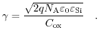 |
(7.47) |
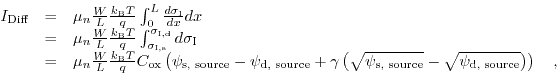
Knowing all needed relations, the integrations for the drain current can be performed. Starting with the determination of the diffusive part of the current,
 |
(7.48) |
and followed by the drift part of the drain current,
![\begin{displaymath}\begin{array}{ccl} I_{\text{Drift}} &=& -\mu_{n} \frac{W}{L} ...
...}-\psi_{\text{s, source}}^{3/2}\right)\right]\quad, \end{array}\end{displaymath}](img1045.png) |
(7.49) |
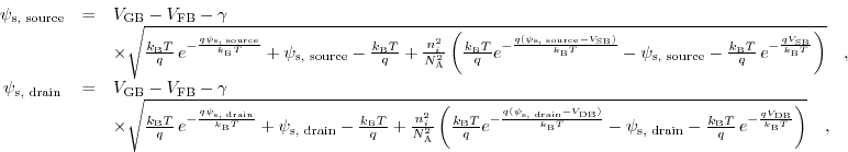
one completes the equation system. The surface potentials
 and
and
 can be determined by iterating the subsequent equations:
 |
(7.50) |
where
 and
and
 denote the source and drain biases with respect to the bulk, respectively.
Next: Bibliography
Up: Appendix
Previous: D. Relation Between Charge
T. Windbacher: Engineering Gate Stacks for Field-Effect Transistors