|
A possible alternative channel material for future electronic devices is the use of silicon NanoWires (NW). Silicon NWs have attracted significant attention as efficient electronic and thermoelectric devices after the realization that length scale provides an additional degree of freedom in engineering their electronic and thermal transport properties. Thermoelectric devices traditionally operate on low efficiency. Nanostructured thermoelectric devices with enhanced performance compared to their bulk counterparts, however, have recently been realized. Silicon NWs with performance two orders of magnitude higher than that of bulk silicon have been demonstrated.
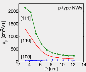
We use the atomistic tight-binding sp3d5s*-SO model and Boltzmann transport theory with all relevant scattering mechanisms included, to investigate the transport properties of silicon NWs. We studied the effect of physical quantization on the electronic structure of NW channels and identified the main electronic structure factors that influence their performance. It was found that structural quantization below 10nm can severely affect the electronic properties of NW channels by changing the effective masses, changing the curvature of the bands, and altering degeneracies through valley and subband splitting. Different wire orientations have different transport properties. This length and orientation degree of freedom in engineering silicon NW channels offers optimization possibilities for nanostructured electronic and thermoelectric devices. It was found that [100] oriented NWs are beneficial for electron transport for the larger NW diameters. As the diameter decreased, however, the [110] NWs performed better. For hole transport, the [111] and secondly the [110] NWs performed better, whereas the [100] NWs are the worst in terms of their transport properties. Furthermore, as the diameter is reduced down to 3nm, the mobility of the [111] and [110] NWs increases by almost 8X, as shown in the figure. This behavior originates from confinement induced large curvature variations in the subbands of these NWs. It demonstrates how the length scale degree of freedom can be utilized to improve the electronic and thermoelectric properties of nanoscale devices.
|