|
|
|
|
||
| Previous: 3.1.6 Metal-Semiconductor Contacts Up: 3.1.6 Metal-Semiconductor Contacts Next: 3.1.6.2 Schottky Contact | ||||
|
|
|
|
||
| Previous: 3.1.6 Metal-Semiconductor Contacts Up: 3.1.6 Metal-Semiconductor Contacts Next: 3.1.6.2 Schottky Contact | ||||
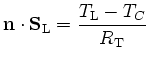
| (3.30) |
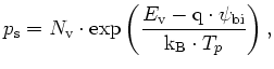
 |
(3.31) |
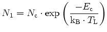 |
(3.32) |
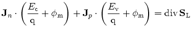
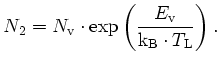 |
(3.33) |
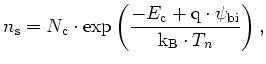 |
(3.34) |
 |
(3.35) |
 |
(3.39) |