|
|
|
|
Previous: 3.1.6.1 Ohmic Contact Up: 3.1.6 Metal-Semiconductor Contacts Next: 3.1.6.3 Polysilicon Contact |
|
|
|
|
Previous: 3.1.6.1 Ohmic Contact Up: 3.1.6 Metal-Semiconductor Contacts Next: 3.1.6.3 Polysilicon Contact |
![\includegraphics[width=0.5\linewidth]{figures/schottky_contact.eps}](img308.png)
|
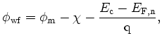 |
(3.42) |
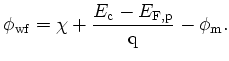 |
(3.43) |
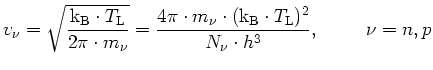 |
(3.47) |
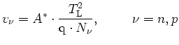 |
(3.48) |
 |
(3.49) |
 |
(3.50) |
 |
(3.51) |
![$\displaystyle J_n = \frac{4\pi{\mathrm{q}}\cdot m_n \cdot ({\mathrm{k_B}}\cdot ...
...hi_\mathrm{m}}{{\mathrm{k_B}}\cdot T_\mathrm{L}} \right) - 1\right]\hspace{5mm}$](img325.png) |
(3.52) |
![$\displaystyle J_p = - \frac{4\pi{\mathrm{q}}\cdot m_p \cdot ({\mathrm{k_B}}\cdo...
...}}\cdot \phi_\mathrm{Bp}}{{\mathrm{k_B}}\cdot T_\mathrm{L}} \right) - 1\right].$](img326.png) |
(3.53) |
|
|
|
|
Previous: 3.1.6.1 Ohmic Contact Up: 3.1.6 Metal-Semiconductor Contacts Next: 3.1.6.3 Polysilicon Contact |
![\includegraphics[width=0.5\linewidth]{figures/work_function.eps}](img311.png)