|
|
|
|
||
| Previous: 2.2 Wafer Description Up: 2.2 Wafer Description Next: 2.2.2 Operations on the Wafer Data | ||||
|
|
|
|
||
| Previous: 2.2 Wafer Description Up: 2.2 Wafer Description Next: 2.2.2 Operations on the Wafer Data | ||||
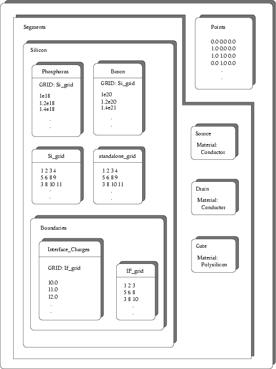
There are two representations of the Wafer data. One comprises objects that are stored in memory (core data structures), in the second representation data are stored persistently on a disk. Fig. 2.1 depicts the persistent data representation of a Wafer.
The Points section contains the coordinates of all points of the wafer, it is a global list of points. All grid elements share this point list. This prevents the storage of redundant coordinate information.
The segments section may contain an arbitrary number of so-called stand-alone grids and also an arbitrary number of attributes, boundaries and properties. Attributes are used to store distributed quantities. A distributed quantity is always defined on a grid, by defining a value for each grid point. The list of attribute values is separated from the grid. This makes it possible that one grid is shared among an arbitrary number of attributes. Properties are like attributes but do not reference a grid. They are constant over the whole segment. Properties are used to store information like the material type of a segment. Stand-alone grids are optional in case at least one distributed quantity is defined on the segment, but must be present (to define the geometry of a segment) otherwise. A segment that consists only of the pure geometry information might be created from a topography simulator or from any kind of geometry modeling tool. A boundary holds an optional number of attributes and properties. Logically, boundaries are contained in a segment and define a part or the whole hull of a segment. Fig. 2.2(a) and Fig. 2.2(b) depict the geometry and a boundary conforming grid of an example Wafer.
![\begin{figure}\centering\subfigure[Geometry of HBT device] {\psfig{file=pics/hbt...
...vice] {\psfig{file=pics/grid, angle=-90, width=0.45\linewidth}}
\par\end{figure}](img16.png) |
|
|
|
|
||
| Previous: 2.2 Wafer Description Up: 2.2 Wafer Description Next: 2.2.2 Operations on the Wafer Data | ||||