There are three major questions to be answered by TCAD regarding electromigration reliability issues. First, interconnect layout designers need to know, how long a drafted interconnect structure will work properly, e.g. for the given operating conditions, how long does it take for complete electromigration failure to happen. The second question of interest is, how does the interconnect resistance change due to electromigration damage. And, the third interesting question is how does the local picture of all electromigration promoting factors looks like in the case when electromigration damage takes place.
The thorough knowledge of the physical phenomena behind the electromigration failure and the capability to model and simulate these phenomena is the only way to accomplish interconnect layouts which optimally meet technology requirements and at the same time avoid far to restrictive design rules.
In the following sections we will present application of the introduced physical models and numerical concepts, realized in the simulation tools, on the different aspects of the electromigration reliability problem.
In all following simulations a circle was chosen as initial void shape. The
resolution of the parameter ![]() profile can be manipulated by setting
parameter
profile can be manipulated by setting
parameter ![]() which is the mean number of triangles across
the void-metal interface. On Fig. 4.8 initial grids for
which is the mean number of triangles across
the void-metal interface. On Fig. 4.8 initial grids for ![]() and
and
![]() are presented.
are presented.
|
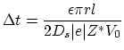 |
(4.60) |
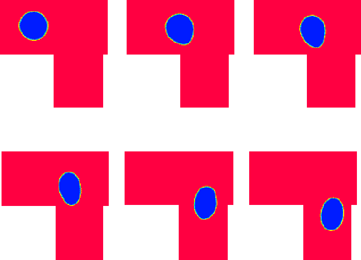
An initial void with some small radius ![]() is placed at some characteristic position inside the three-dimensional interconnect structure (Figure 4.15). Since most of the fatal voids are nucleated in the vicinity or in the area of interconnect vias we consider in particular these cases. The configurable initial void volume is
is placed at some characteristic position inside the three-dimensional interconnect structure (Figure 4.15). Since most of the fatal voids are nucleated in the vicinity or in the area of interconnect vias we consider in particular these cases. The configurable initial void volume is ![]() which is smaller than
which is smaller than
![]() because the void area is confined by sphere and boundary of the interconnect (Figure 4.15).
Starting from the initial void radius
because the void area is confined by sphere and boundary of the interconnect (Figure 4.15).
Starting from the initial void radius ![]() , the void radius is gradually incremented
, the void radius is gradually incremented
![]() , with
, with
![]() .
For each void radius the electrical field in the interconnect structure is calculated by means of the finite element method using a diffuse interface approach.
To obtain the distribution of the electrical potential inside the interconnects the Poisson equation (4.50) has to be solved.
.
For each void radius the electrical field in the interconnect structure is calculated by means of the finite element method using a diffuse interface approach.
To obtain the distribution of the electrical potential inside the interconnects the Poisson equation (4.50) has to be solved.
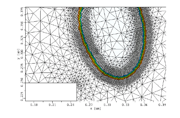
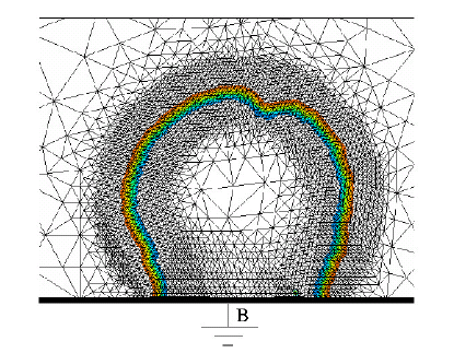
In order to obtain sufficient accuracy the scalar field
![]() must be resolved on a locally refined mesh (Figure 4.16).
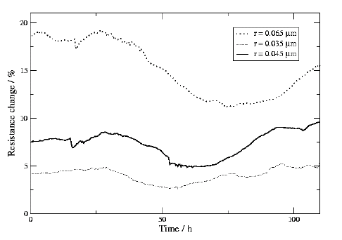
For an electrical field calculated in such a way, the resistance of the interconnect via is also calculated [76,91]. With growing void size the resistance increases. The whole process is stopped when a void radius is reached for which
must be resolved on a locally refined mesh (Figure 4.16).
For an electrical field calculated in such a way, the resistance of the interconnect via is also calculated [76,91]. With growing void size the resistance increases. The whole process is stopped when a void radius is reached for which
![]() .
.
|
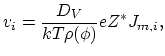
The primary driving force of material transport at the void surface is electromigration proportional to the tangent component of the vector current density. Since the diffuse interface approach for the calculation of the current density ensures physical behavior of the electrical field in the vicinity of the isolating void, the normal component of the current density on the void surface is always zero and we can apply the formula
|
The evolution of the void is caused by material transport on the void surface and in the vicinity of the void surface. The mass conservation law gives the mean propagation velocity ![]() of the evolving void-metal interface
of the evolving void-metal interface
As we can see from Figure 4.17, the average current density on the void surface increases with the void size. Both, current density and resistance, exhibit a very similar dynamic behavior. The dynamical resistance increase is in accordance with the measurement results presented in [52]. Compared with the earlier result [92], which assumes cubical void shapes, our approach enables more realistic simulations. An open question is how to use the obtained average current density (Figure 4.17) for the estimation of the void growing time (
As we can see from (
![]() ), the velocity
), the velocity ![]() depends on the vacancy diffusivity
depends on the vacancy diffusivity ![]() which itself has significantly varying values depending on the diffusion path.
The electromigration assisted self-diffusion of copper is a complex process which includes simultaneous diffusion through the crystal bulk, along grain boundaries, along the copper/barrier interfaces, and along the copper/cap-layer interface.
Therefore, the diffusivity applied in (
which itself has significantly varying values depending on the diffusion path.
The electromigration assisted self-diffusion of copper is a complex process which includes simultaneous diffusion through the crystal bulk, along grain boundaries, along the copper/barrier interfaces, and along the copper/cap-layer interface.
Therefore, the diffusivity applied in (
![]() ) must be a cumulative value (see equation 4.12).
For a feasible estimation of
) must be a cumulative value (see equation 4.12).
For a feasible estimation of ![]() , reliable, experimentally determined values for all relevant diffusivities are needed and these are until now unfortunately not available [55,8].
, reliable, experimentally determined values for all relevant diffusivities are needed and these are until now unfortunately not available [55,8].
In this section we present the simulation of the influence of electromigration promoting factors on the electromigration behavior for the case of a complex interconnect structure produced with advanced process simulation tools.
The results of the transient electro-thermal simulation (Section 4.3.2) are used to setup a thermo-mechanical (Section 4.3.2) and material transport simulation. The model applied is similiar to that presented in Section 4.4.5 but without taking into account the connection between the local vacancy dynamic and overall mechanical stress distribution.
An effective vacancy diffusivity is chosen assuming the copper/TiN barrier interface as the dominant diffusion path [55].
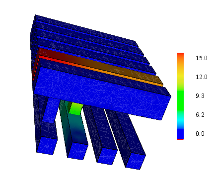
An interconnect structure with 6 metal (copper) lines crossing 4 other lines at a
lower level and connected with vias/contacts was generated using a typical
damascene process flow.
This was performed by using a combination of DEP3D [93] (only for deposition of TiN barrier
layer and copper deposition for the second metal layer and for dielectric deposition
of the topmost layer) with DEVISE [94] (used for emulating the other deposition,
etching and polishing steps).
The barrier layer is 0.02 ![]() m thick; each metal line in the first layer is 3
m thick; each metal line in the first layer is 3 ![]() m long with a width of 0.25
m long with a width of 0.25 ![]() m and aspect ratio of 1.2.
For the second layer, each metal line is 2.2
m and aspect ratio of 1.2.
For the second layer, each metal line is 2.2 ![]() m long with a width 0.3
m long with a width 0.3 ![]() m and aspect ratio 1.5.
The contacts/vias have a width of 0.2
m and aspect ratio 1.5.
The contacts/vias have a width of 0.2 ![]() m with an aspect ratio of 2.5.
The dielectric medium surrounding the metal lines is silicon-dioxide.
The contacts for electrical characterization were defined using DEVISE.
m with an aspect ratio of 2.5.
The dielectric medium surrounding the metal lines is silicon-dioxide.
The contacts for electrical characterization were defined using DEVISE.
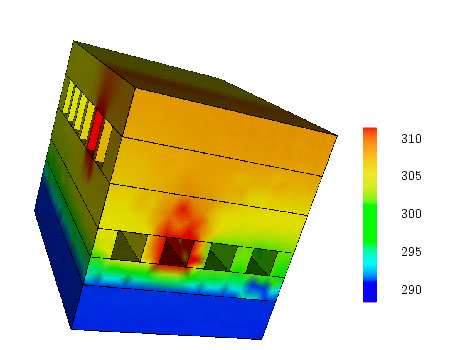
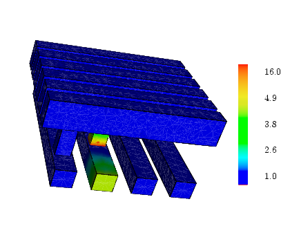
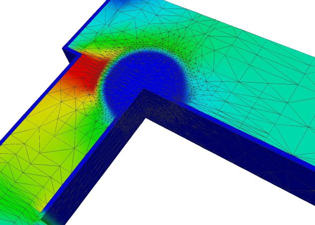
The simulation of the electro-thermal problem was carried out with the SAP [91] tool and the simulation of mechanical stress and electromigration problem with FEDOS tool. The simulation results are presented in the Figure 4.18 - Figure 4.20. We can see in Figure 4.18 electrical potential distribution. The gradient of the electrical potential determines direction and intensity of the electromigration driving force.
The corresponding temperature distribution is presented in Figure 4.19. The temperature has twofold influence on the electromigraton. First, temperature changes diffusion coefficeints on all diffusion paths according to Arrhenius' law. Secondly, for the case that due to specific interconnect layout and operating conditions a substantial gradients in the temperature distribution are available, these gradients represents additional driving force which can promote or opose electromigration (4.32). Additionally, thermal mismatch between copper, barrier and silicon-dioxide passivation layer causes a build-up of thermo-mechanical stress.
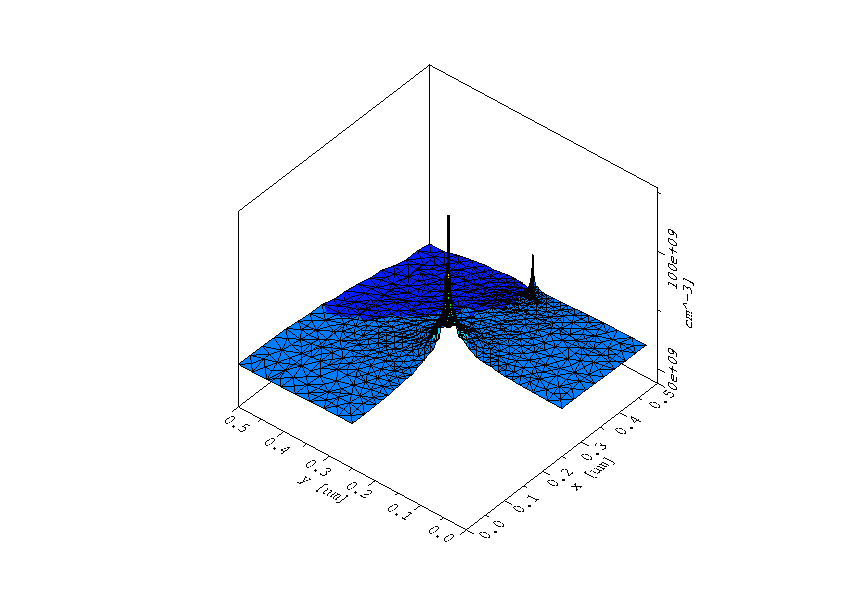
The peak values of the vacancy concentration indicate the spots where serious material transport discontinuity takes place. These hot spots are the locations where the void nucleation can be expected (Figure 4.20). Analysis of the experimental results [55,95,77] shows that the material transport discontunity can be intialised by the geometrical properties of layout itself, like in the cases where the segments of the copper interconnects are divided by barrier layer, and promoted due to electromigration unbalanced by other driving fources. A significant part plays also the grain boundary structure of the copper acting as a network of fast diffusivity paths.
During the operating of an interconnect generally the redistribution of vacancies under the influence of the promoting factors takes place. Starting from the uniformly distributed vacancies, during the operating of the interconnect local peaks of the vacancy concentration are built (Figure 4.20).
If the balance of promoting factors and temperature gradients which characterize operating conditions of the interconnect is reached, the vacancy concentration will remain at some
value independent of the simulation duration: the interconnect structure is virtually
immortal.
However, if the electrical field is so high that electromigration overrides the material reaction presented through concentration and mechanical stress gradients, the vacancy concentration will increase steadily and at some point (e.g. vacancy concentration reaches unrealistic high values) the applied model is no more valid.
If the vacancy concentration is higher than the lattice sites concentration throughout some volume of the macroscopic dimensions (for example ![]() of the interconnect width), we can assume that void is already nucleated and for further simulation void evolution models should be applied (Sections 4.6.1 and 4.6.2).
The interconnect layout and operating conditions choosen in our simulation example produce a situation where the vacancy concentration remains stable at
of the interconnect width), we can assume that void is already nucleated and for further simulation void evolution models should be applied (Sections 4.6.1 and 4.6.2).
The interconnect layout and operating conditions choosen in our simulation example produce a situation where the vacancy concentration remains stable at
![]() cm
cm![]() and under the lattice sites concentration (
and under the lattice sites concentration (![]() cm
cm![]() ).
).
|
![\includegraphics[height=0.4\linewidth]{figures/init_n_1.eps}](img885.png)
![\includegraphics[height=0.4\linewidth]{figures/init_n_5.eps}](img886.png)
![\includegraphics[height=0.4\linewidth]{figures/via.eps}](img887.png)
![\includegraphics[width=0.3\linewidth]{figures/void2.eps}](img904.png)
![$\displaystyle J_{m,i}=2\frac{\int_{V}\Vert\mathbf{J}\Vert[1-\phi^2_i(x,y,z)] dV}{\int_{V}[1-\phi^2_i(x,y,z)] dV},$](img905.png)
![\includegraphics[width=0.6\textwidth]{figures/tmpPlot2.eps}](img913.png)