|
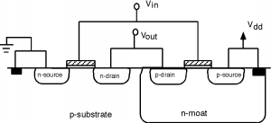
The p-channel MOSFET relies on an n-type substrate. As commonly p-type wafers are used for processing, an additional n-type well implant is necessary. In this well, which is a deep region of n-type doping, the p-channel MOSFET is placed. As the p-substrate and the n-well junction is reverse biased, no significant current flows between these regions and the two transistors are isolated.
The output current of the p-channel MOSFET is typically much lower than the
current of an n-channel MOSFET with similar dimensions and dopings. This is
due to the lower carrier mobility of holes compared to electrons. As the
characteristics of the complementary transistors should be as equal as
possible, the width of the p-channel MOSFET is typically made larger to
compensate the difference. In our example device the necessary geometry factor
is ![]() to obtain equal drain currents for equal gate biases.
to obtain equal drain currents for equal gate biases.
![\includegraphics[width=8cm]{figures/cmos-inverter-circuit}](img640.png)
|
Considering negative bias temperature instability, the worst stress conditions
are imposed on the p-channel MOSFET at
![]() . At this bias
condition the pMOSFET is turned on, with approximately the same potential at
the source and the drain
. At this bias
condition the pMOSFET is turned on, with approximately the same potential at
the source and the drain
![]() and negative gate to substrate
voltage
and negative gate to substrate
voltage
![]() .
.
The gate-source voltage
![]() of the n-channel MOSFET is equal to
of the n-channel MOSFET is equal to
![]() while
the gate-source voltage of the p-channel MOSFET calculates as
while
the gate-source voltage of the p-channel MOSFET calculates as
| (7.1) |
| (7.2) |
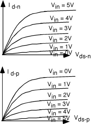
Looking at the output characteristics of the two transistors
(Figure 7.12), and considering that the drain currents,
![]() , of
both transistors must be equal, the voltage transfer characteristic can be
extracted, as seen on Figure 7.13. From this figure it is obvious
that a shift of the output characteristics of one transistor can have big
impact especially around the turn-over point of the VTC.
, of
both transistors must be equal, the voltage transfer characteristic can be
extracted, as seen on Figure 7.13. From this figure it is obvious
that a shift of the output characteristics of one transistor can have big
impact especially around the turn-over point of the VTC.
|
|
The mixed-mode of Minimos-NT allows to simulate the whole circuit while the device characteristics for each device are solved using the semiconductor device equations. Thus, the degradation of the p-channel MOSFET due to negative bias temperature instability can be accounted for in the circuit simulation.
![\includegraphics[width=\figwidth]{figures/cmos-inverter_fullsweep}](img649.png)
|
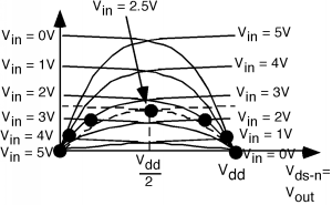
NBT stress has its highest impact on the p-channel MOSFET during low input
![]() . At this condition the transistor has a gate to substrate
voltage of approximately
. At this condition the transistor has a gate to substrate
voltage of approximately
![]() . When the circuit is additionally subject to
thermal stress, then the threshold voltage of the p-channel transistor is
degraded. As the n-channel device has a much lower susceptibility to this type
of stress (Section 6.3.7), the circuit loses its symmetry. As
shown in Figure 7.15, is the switching point of the output potential
moved to a lower input voltage. An interface trap density
. When the circuit is additionally subject to
thermal stress, then the threshold voltage of the p-channel transistor is
degraded. As the n-channel device has a much lower susceptibility to this type
of stress (Section 6.3.7), the circuit loses its symmetry. As
shown in Figure 7.15, is the switching point of the output potential
moved to a lower input voltage. An interface trap density
![]() , which is already a severely damaged interface
(Chapter 3), reduces the switching point by more than 1V.
, which is already a severely damaged interface
(Chapter 3), reduces the switching point by more than 1V.
![\includegraphics[width=\figwidth]{figures/cmos-vtc-shift}](img653.png)
|
![\includegraphics[width=\figwidth]{figures/cmos-inverter-trans-reverse}](img654.png)
|
![\includegraphics[width=\figwidth]{figures/cmos-inverter-trans}](img655.png)
|
Not only in the stationary case does the degradation influence the circuit performance. Transient simulations show (Figure 7.16 and 7.17) that the switching behavior of a circuit comprising a degraded p-channel MOSFET is different. This must be kept in mind when designing timing-critical CMOS circuits.
At high input,
![]() , the p-channel MOSFET is turned off and the
n-channel device turned on, pulling the output voltage to ground,
, the p-channel MOSFET is turned off and the
n-channel device turned on, pulling the output voltage to ground,
![]() . Switching to
. Switching to
![]() turns off the n-channel device and on the
p-channel device. The switching speed depends on the magnitude of the gate
overdrive,
turns off the n-channel device and on the
p-channel device. The switching speed depends on the magnitude of the gate
overdrive,
![]() . An NBT degraded pMOS transistor has a lower (more
negative) threshold voltage, therefore a lower gate overdrive and is turned on
slower. The result is a slower CMOS inverter when turning the output
. An NBT degraded pMOS transistor has a lower (more
negative) threshold voltage, therefore a lower gate overdrive and is turned on
slower. The result is a slower CMOS inverter when turning the output
![]() , as seen in Figure 7.16.
, as seen in Figure 7.16.
The opposite case, turning the inverter from
![]() to
to
![]() is completely different, as seen in Figure 7.17. Here, the
p-channel transistor is switched from on to off. In this case the gate
overdrive equals the magnitude of the threshold voltage. The degraded device,
with its more negative
is completely different, as seen in Figure 7.17. Here, the
p-channel transistor is switched from on to off. In this case the gate
overdrive equals the magnitude of the threshold voltage. The degraded device,
with its more negative
![]() is driven into stronger inversion and can, thus,
be turned off more quickly.
is driven into stronger inversion and can, thus,
be turned off more quickly.
![\includegraphics[width=0.495\textwidth]{figures/cmos-n-outputchar}](img648.png)