


Next: 7.4 Ring Oscillator
Up: 7. Case Studies
Previous: 7.2 CMOS Inverter
Subsections
Figure 7.18:
Circuit of a 6 transistor SRAM cell. It consists of two CMOS
inverters and two access MOSFETs. NBT stress mainly affects the p-channel
transistors.
|
|
Static random access memory (SRAM) can retain its stored information as long as
power is supplied. This is in contrast to dynamic RAM (DRAM) where periodic
refreshes are necessary or non-volatile memory where no power needs to be
supplied for data retention, as for example flash memory. The term ``random
access'' means that in an array of SRAM cells each cell can be read or written
in any order, no matter which cell was last accessed.
The structure of a 6 transistor SRAM cell, storing one bit of information, can
be seen in Figure 7.18. The core of the cell is formed by two CMOS
inverters, where the output potential of each inverter
 is fed as input
into the other
is fed as input
into the other
 . This feedback loop stabilizes the inverters to their
respective state.
. This feedback loop stabilizes the inverters to their
respective state.
The access transistors and the word and bit lines, WL and BL, are used to read
and write from or to the cell. In standby mode the word line is low, turning
the access transistors off. In this state the inverters are in complementary
state. When the p-channel MOSFET of the left inverter is turned on, the
potential
 is high and the p-channel MOSFET of inverter two is turned
off,
is high and the p-channel MOSFET of inverter two is turned
off,
 is low.
To write information the data is imposed on the bit line and the inverse data
on the inverse bit line,
 . Then the access transistors
are turned on by setting the word line to high. As the driver of the bit lines
is much stronger it can assert the inverter transistors. As soon as the
information is stored in the inverters, the access transistors can be turned
off and the information in the inverter is preserved.
. Then the access transistors
are turned on by setting the word line to high. As the driver of the bit lines
is much stronger it can assert the inverter transistors. As soon as the
information is stored in the inverters, the access transistors can be turned
off and the information in the inverter is preserved.
For reading the word line is turned on to activate the access transistors while
the information is sensed at the bit lines.
Figure 7.19:
Static noise margin (SNM) of the unstressed SRAM cell. The window
in the ``butterfly'' curve illustrates the hardiness against DC noise.
|
|
A key figure of merit for an SRAM cell is its static noise margin (SNM). It
can be extracted by nesting the largest possible square in the two voltage
transfer curves (VTC) of the involved CMOS inverters, as seen in
Figure 7.19. The SNM is defined as the side-length of the square, given
in volts. When an external DC noise is larger than the SNM, the state of the
SRAM cell can change and data is lost.
The effect of NBTI impacts one or both p-channel MOSFETs in the SRAM cell,
depending on the charge state during temperature stress. The result is a
degraded VTC and, therefore, a degraded SNM.
Figure 7.20:
Degradation of one p-channel MOSFET in an SRAM cell. An interface
trap density
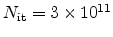 cm
cm causes read failure even at
zero noise.
causes read failure even at
zero noise.
|
|
Figure 7.20 shows the impact of NBTI on an SRAM cell. Here, only
one of the p-channel MOSFETs is degraded. This is the typical situation when
the information stored in the cell does not change frequently. An interface
trap density of
 is enough to drastically
reduce the SNM. At
is enough to drastically
reduce the SNM. At
 the window
completely disappears and the SRAM cell loses its functionality.
the window
completely disappears and the SRAM cell loses its functionality.
Figure 7.21:
Degradation of both p-channel MOSFET in an SRAM cell. The original
``butterfly'' curve is completely degenerated.
|
|
Assumed degradation of both p-channel MOSFETs results in shift of the VTCs of
both inverters (Figure 7.21). This leads to a complete
degeneration of the original VTCs.
Next: 7.4 Ring Oscillator
Up: 7. Case Studies
Previous: 7.2 CMOS Inverter
R. Entner: Modeling and Simulation of Negative Bias Temperature Instability
![\includegraphics[width=16cm]{figures/sram-circuit}](img658.png)
![\includegraphics[width=\figwidth]{figures/sram-vtc}](img662.png)
![\includegraphics[width=\figwidth]{figures/sram-vtc-shift}](img663.png)
![\includegraphics[width=\figwidth]{figures/sram-vtc-shift-both}](img666.png)