The problem is treated one-dimensionally in this section. Even with
drain-source bias we assume that the gradual-channel-approximation (G.C.A.)
remains valid in the channel and that the field perpendicular to the interface
is much larger than the field parallel to the interface ([164]).
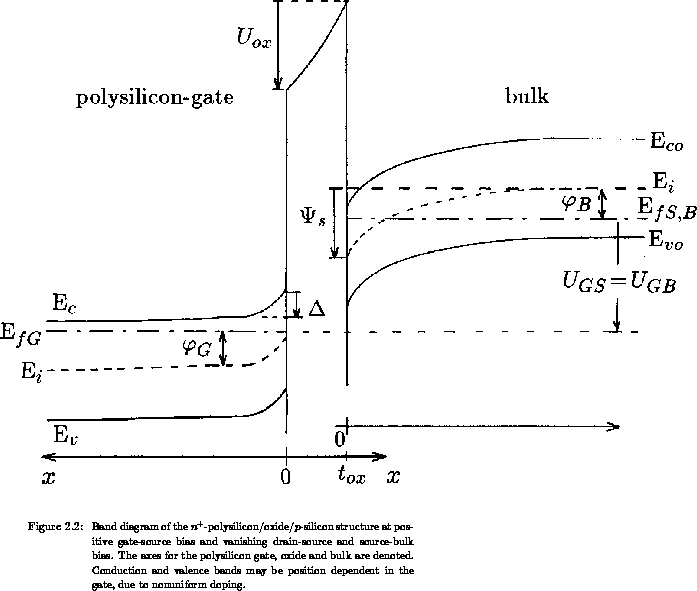
Figure 2.2 shows the  -polysilicon-gate/oxide/
 -silicon
structure at positive gate bias and vanishing drain-source and bulk-source
voltages. The applied gate-bulk voltage is distributed on the gate, oxide and
bulk. The basic phenomenological equation describing the interaction between
the polysilicon gate and the bulk is given by the Gauss law
-silicon
structure at positive gate bias and vanishing drain-source and bulk-source
voltages. The applied gate-bulk voltage is distributed on the gate, oxide and
bulk. The basic phenomenological equation describing the interaction between
the polysilicon gate and the bulk is given by the Gauss law
where  is the transversal surface field in the gate at the gate/oxide
interface and
is the transversal surface field in the gate at the gate/oxide
interface and  is the transversal surface field in the bulk. Remark that
 . Roughly speaking, the same surface
field appears on both sides of the oxide. Since can
be very high in (submicrometer) thin-oxide devices, it follows that
can be high too, leading to a non-negligible voltage drop in the gate,
even when the gate is heavily doped. The permittivity
. Roughly speaking, the same surface
field appears on both sides of the oxide. Since can
be very high in (submicrometer) thin-oxide devices, it follows that
can be high too, leading to a non-negligible voltage drop in the gate,
even when the gate is heavily doped. The permittivity  and
and
 refer to silicon bulk and polysilicon gate, respectively. Due
to heavy-doping effects, the permittivity of the heavily doped polysilicon may
differ from the permittivity of the undoped silicon, as explained
in [165] and references cited in this paper.
refer to silicon bulk and polysilicon gate, respectively. Due
to heavy-doping effects, the permittivity of the heavily doped polysilicon may
differ from the permittivity of the undoped silicon, as explained
in [165] and references cited in this paper.
The charges  and
and  reside at the gate/oxide and oxide/bulk
interface, respectively. In contrast to many studies dealing with
fixed oxide charge and traps at the interface of thermally oxidized
single-crystal silicon [331], much less attention has been paid in
literature to study the polysilicon/oxide interface for polysilicon
deposited over oxide or oxidized polysilicon. While the oxide/bulk interface
is of significant technological importance, the gate/oxide interface never
had an impact on MOS device characteristics.
It has been suggested in [520][274] that electron-trapping
interface states exist at the polysilicon-gate/oxide interface. A positive
consisting of interface trapped charge and/or fixed oxide charge of
order
reside at the gate/oxide and oxide/bulk
interface, respectively. In contrast to many studies dealing with
fixed oxide charge and traps at the interface of thermally oxidized
single-crystal silicon [331], much less attention has been paid in
literature to study the polysilicon/oxide interface for polysilicon
deposited over oxide or oxidized polysilicon. While the oxide/bulk interface
is of significant technological importance, the gate/oxide interface never
had an impact on MOS device characteristics.
It has been suggested in [520][274] that electron-trapping
interface states exist at the polysilicon-gate/oxide interface. A positive
consisting of interface trapped charge and/or fixed oxide charge of
order  or less has been detected by HF
  -
- measurements
on polysilicon capacitors in [520]. Studies of a heavily doped
polysilicon/oxide system in [200] have shown several controversial
phenomena which are not clearly understood and which have been
attributed to the dipoles at the gate/oxide interface, positive electron traps
in the oxide near the interface and the positive fixed charge residing deeply
in the oxide. According to [441] increasing the bulk doping increases
the densities of both, fixed charge and interface traps at the interface formed
by thermal oxidation of silicon.
Such a study is still missing, for moderately doped polysilicon deposited over
the oxide thermally grown on silicon, in the literature. In the following we
assume to be fixed charge. In relationship 2.2,
measurements
on polysilicon capacitors in [520]. Studies of a heavily doped
polysilicon/oxide system in [200] have shown several controversial
phenomena which are not clearly understood and which have been
attributed to the dipoles at the gate/oxide interface, positive electron traps
in the oxide near the interface and the positive fixed charge residing deeply
in the oxide. According to [441] increasing the bulk doping increases
the densities of both, fixed charge and interface traps at the interface formed
by thermal oxidation of silicon.
Such a study is still missing, for moderately doped polysilicon deposited over
the oxide thermally grown on silicon, in the literature. In the following we
assume to be fixed charge. In relationship 2.2,
 is the total space charge in the oxide
where  is the oxide-charge density and
  denotes the oxide
thickness. The potential difference on the oxide is given by
denotes the oxide
thickness. The potential difference on the oxide is given by
where  is the oxide capacitance per unit area and
 is the equivalent charge in the oxide
Note that differs from . The ratio is directly dependent
on the distribution. appears only in
relationship 2.2 and may be embedded in the term . The
charge in 2.4 may be absorbed in , as is
usually done.
An eventual dipole layer in the oxide near the gate/oxide interface, speculated
in [200], leads to an additional term  on the
right-hand-side in expression 2.4.
on the
right-hand-side in expression 2.4.  is the dipole
charge with reference positive end oriented towards the gate and
is the dipole
charge with reference positive end oriented towards the gate and  is the
dipole length. Other equations remain unchanged when dipoles are present.
Henceforward, a dipole layer is omitted in the model.
is the
dipole length. Other equations remain unchanged when dipoles are present.
Henceforward, a dipole layer is omitted in the model.
We allow position-dependent band-gap narrowing in the gate. For the structure shown in Figure 2.2 the voltage conversation reads
where  is determined by 2.4.
Relationship 2.6 also includes the substrate back-bias
is determined by 2.4.
Relationship 2.6 also includes the substrate back-bias
 .
.  denotes the potential of the intrinsic level at the
oxide/bulk interface with respect to the intrinsic level deep in the bulk and
denotes the potential of the intrinsic level at the
oxide/bulk interface with respect to the intrinsic level deep in the bulk and
 is the Fermi barrier deep in the bulk.
 is the Fermi barrier in the gate. referred to the
interconnector/polysilicon contact (gate-contact in hence) is given by
is the Fermi barrier in the gate. referred to the
interconnector/polysilicon contact (gate-contact in hence) is given by
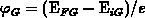 , where
  is the energy
of the Fermi level in the gate controlled by external gate-bias.
is the energy
of the Fermi level in the gate controlled by external gate-bias.  is the energy of the intrinsic level in an ideal silicon band imagined
at the place of the heavily doped gate and measured at the gate-contact
is the energy of the intrinsic level in an ideal silicon band imagined
at the place of the heavily doped gate and measured at the gate-contact
 . The band diagram in the
gate is clarified in Figure 2.3.
. The band diagram in the
gate is clarified in Figure 2.3.  represents the
voltage drop in the polysilicon gate, i.e. the negative potential at the
gate/oxide interface with respect to
represents the
voltage drop in the polysilicon gate, i.e. the negative potential at the
gate/oxide interface with respect to  level at the same point where
is being defined. When is associated with the
gate-contact, includes the total potential difference laying on the
gate due to both, electric-field penetration into the gate () and the
potential variation with the inhomogeneity in the gate-doping.
level at the same point where
is being defined. When is associated with the
gate-contact, includes the total potential difference laying on the
gate due to both, electric-field penetration into the gate () and the
potential variation with the inhomogeneity in the gate-doping.
We restricted ourselves to the steady-state in the present model, although some
transient effects may well be expected in nondegenerately doped gates
(cf. Section 2.4). In the steady-state a thermodynamic
quasi-equilibrium holds in the gate; net recombination vanishes and leakage
currents are negligible. A unique and constant Fermi level of both, electrons
and holes exists in the gate, as opposed to the bulk where electron and hole
Fermi levels are splitted when  and/or
  are nonzero.
For the selfconsistent solution of the system 2.2-2.6, it is necessary to establish the relationships between the surface field and the surface potential in both, gate and bulk. These relationships depend only on the physical model and doping profile in the particular material.