
The first part of this work will be devoted to the characterization of preexisting defects in Silicon metal-oxide-semiconductor field-effect transistors (MOSFETs), and evaluation of their lateral positions. This study requires both modeling of charged carrier transport through the device channel in the presence of random dopants and single defects, and experimental analysis. Information on main simulation and experimental techniques used will be provided within this chapter.
The channel of modern Silicon MOSFETs typically presents a multi-particle system with randomly distributed dopants and defects. This system can be described by the time-dependent Schroedinger equation, which generally reads [14]
|
| (2.1) |
where m0 and M0 are the masses of electrons and ions, respectively. While r expresses the positions of electrons and R the positions of ions, Hee(r), Hii(R) and Hei(r, R) denote electron-electron scattering and the interactions of ions with other ions and electrons, respectively.
However, the solution of the multi-particle Equation 2.1 is extremely complicated. Therefore, by separation of wave functions for electrons and holes, and using Hartree-Fock and Slater approximations [119], it is typically transferred into a single-particle Schroedinger equation for electrons
 | (2.2) |
where Ψ(x, k, t) is the wave function of a single electron, V ext(x, t) is the external electrostatic potential and Hsc(x, k) is a scattering Hamilton operator which combines other interactions between different particles. The quantities k and V (x) denote the reciprocal wave vector and ionic potential [119], respectively. Furthermore, another Hamilton operator
 | (2.3) |
is introduced, where
 | (2.4) |
and Hm(k) presents a dispersion relation in the m-th band, which allows for the inclusion of the full band structure of the semiconductor (i.e. all conduction and valence bands) [119]. This dispersion relation is given by the type of channel material [14].
The single-particle Schroedinger Equation 2.2 can be used to derive the Boltzmann Transport Equation (BTE), which describes electron transport in a semiconductor. While the detailed step-by-step derivation of BTE can be found in [119, 14], in general form this equation reads [14]
 | (2.5) |
where fm(x, k, t) is the carrier distribution function in the m-th band, Q{fm(x, k, t)} is the operator describing scattering processes from a statistical point of view and L{fm(x, k, t)} is a free-streaming operator given as
 | (2.6) |
Here vgrm(x, k) is the group velocity in the m-th band and F(x, t) is an external force given by the gradient of V ext(x, t) from Equation 2.2.
Thus, BTE describes both electron scattering by Q{fm(x, k, t)} and free transport of electrons in between scattering events by L{fm(x, k, t)}, and can be written for any of the conduction or valence bands. A self-consistent solution of the BTE for electrons and holes coupled with the Poisson equation allows for a detailed analysis of charged carrier transport through the MOSFET channel. However, discretization of the original BTE 2.5 leads to a multidimensional system of equations which requires significant computational resources. Therefore, most typically used carrier transport models are obtained by simplification of this system. This can be done using the method of moments [162]. This method denotes jth-order moments of the carrier distribution function f(x, k, t) as
 | (2.7) |
with χj being the jth-order weight function. Hence, using χ 1 = 1 leads to the first moment of the distribution function, which is either electron or hole concentration (n and p, respectively). The second moment is obtained by using χ2 = k and denotes the average drift velocity of carriers ⟨vn⟩ = Jn/q or ⟨vp⟩ = Jp/q, with Jn and Jp being the current density for electrons and holes, respectively. Weighting of the distribution function with χ3 = E(k) leads to the third moment, which presents the average energy for electrons (⟨En⟩) or holes (⟨Ep⟩). Although the higher order moments can be obtained in a similar manner, these first three are typically enough for the derivation of the most widely used carrier transport models.
The drift-diffusion (DD) model is one of the carrier transport models that can be derived from BTE using the method of moments. The main equations of the DD model are the continuity equations for electrons and holes
 | (2.8) |
 | (2.9) |
which present the first two moments of the BTE, and the Poisson equation
 | (2.10) |
Here R is the recombination rate, ε is the dielectric constant and C denotes the concentration of fixed charges. The unknown quantities are the carrier concentrations n and p and the electrostatic potential ψ, while the electron and hole current densities are given by
 | (2.11) |
 | (2.12) |
where the drift term is associated with the electric field F and the diffusion term is given by the concentration gradient. μn, μp and Dn, Dp are the electron and hole mobilities and diffusion coefficients, respectively.
Since the DD model incorporates only the first two moments of the BTE, it can not capture energy transport. Nevertheless, the self-consistent solution of equations 2.8- 2.10 allows for a reliable description of charged carrier transport through the device channel at reasonable computational costs. Therefore, the DD model is typically employed to reproduce the device electrostatics for its implementation into reliability models, especially when studying bias-temperature instabilities [60, 15].
The DD model is incorporated into our deterministic TCAD simulator Minimos-NT [83], which will be used when performing simulations of the output characteristics of Si MOSFETs and when studying the impact of single defects on their performance. Also, an attempt to extend the DD model for the case of graphene FETs will be made within this work, although without implementation into professional simulation software.
It should be noted that some more complex models, e.g. the hydrodynamic transport model employing three moments of the BTE, are also incorporated into Minimos-NT [83]. However, their consideration is beyond the scope of this work.
The Poisson equation 2.10 generally accounts for all charged particles in the device channel by regarding their macroscopic densities (e.g. the density of ionized impurities is described by their concentration C). However, this approach is only applicable for Si MOSFETs with large enough channel lengths. At the same time, for nanoscale MOSFETs with channel lengths of around 100nm and smaller, the amount of charged impurities can be small [9, 11, 153]. Hence, one has to deal with randomly distributed discrete dopants [15], which for brevity can be denoted as “random dopants”. They can originate, for example, from doping of semiconductor substrates using ion implantation.
In nanoscale devices, random dopants can severely impact the channel electrostatics, which are one of the main sources of device-to-device variability [9]. Namely, they can perturb the channel potential [9] and form a percolation path for the current[15]. This leads to different values of the threshold voltage V th for nominally identical devices with different configurations of random dopants. Hence, accounting for the impact of random dopants on the device electrostatics is extremely important when simulating charge carrier transport through the channel. As will become clear from the analysis below, this is the key figure of merit for the characterization of preexisting defects in nanoscale MOSFETs and evaluation of their lateral positions.
Placement of random dopants into the device channel is typically done by discretizing the macroscopic channel doping concentrations (ND for n-MOSFET or NA for p-MOSFET) and using the Monte Carlo algorithm [187] to calculate the position of each particular dopant (details can be found in [14]). However, the accuracy of this method is strongly dependent on the mesh spacing of the simulation grid used. Nevertheless, the authors of [9, 11] have shown that a spacing smaller than 1nm is typically sufficient to capture the magnitude of device-to-device variability in nanoscale MOSFETs.
A randomly placed dopant presents a point charge with the Coulomb potential, which can be screened by numerous carriers having discrete energies [14]. Hence, a classical or semi-classical description would lead to a failure of numerical solution for the Poisson equation. Therefore, modeling of random dopants using a semi-classical simulator incorporating the DD model typically requires accounting for a quantum correction of the Coulomb potential. The most suitable methodology for this is the density gradient (DG) model [9, 11, 184, 19], which allows to obtain quantum corrected drift-diffusion equations (see [14]).
Another source of device-to-device variability in nanoscale MOSFETs is associated with charged traps [121], which also have a discrete distribution along the channel. Their electrostatical interactions with random dopants can lead to variations of the threshold voltage, while the proximity of a charged trap to the dominating percolation path formed by random dopants strongly impacts the drain current [15]. In the course of this work we perform our simulations either for perturbed device with a single discrete trap placed right at the channel/oxide interface or for unperturbed device.
The channel of a modern nanoscale MOSFET contains a number of preexisting defects introduced during fabrication. Charging/discharging of these defects may significantly impact device reliability and also lead to a time-dependent variability [167]. Hence, characterization of preexisting defects is extremely important.
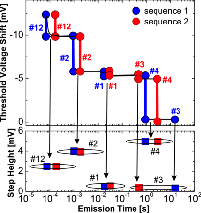
Time-dependent defect spectroscopy (TDDS) [67, 68, 181] is one of the most versatile methods for characterization of individual defects in nanoscale MOSFETs. The typical TDDS experiment includes charging of traps at a higher gate voltage followed by their discharging at a lower voltage. During this the subsequent charge-emission transient is recorded. Multiple repetitions of these charging/discharging sequences allow one to obtain good statistics on capture and emission times for each individual trap.
A typical evolution of the threshold voltage after charging of preexisting defects using TDDS is shown in Figure 2.1. Clearly, the recovery consists of a number of discrete steps, while each of these steps is attributed to discharging of an individual trap. Since this behaviour is reproducible when using subsequent TDDS sequences on the same device, one can extract the corresponding step heights and emission times and build a spectral map (Figure 2.1(bottom))[67]. This spectral map contains unique fingerprints for each of the defects in the device channel. Also, repetition of TDDS measurements at different drain voltages allows for the extraction of ΔV th(V d) characteristics, which will be analyzed within this work. In particular, we will clearly show that the dependence of step height on the drain bias contains the full information on the lateral defect position.