Blocked impurity band (BIB) photo detectors [Stetson86], invented by Petroff and
Stapelbroek [Petroff86], are usually designed for the mid- to far-infrared range from 10
![]() m to 1000
m to 1000 ![]() m wavelength. This wavelength range gained considerable
importance in astronomy since the molecular and atomic emission lines from
species like O, C or
m wavelength. This wavelength range gained considerable
importance in astronomy since the molecular and atomic emission lines from
species like O, C or
![]() are within this range and far away objects
are often hidden by interstellar dust clouds which absorb higher energy
photons. On the other hand the atmosphere filters most of the infrared
radiation and so exploring the infrared spectrum got an significant upturn with
the realization of space based observation facilities such as the Spitzer Space
Telescope where BIB detectors are applied in the form of detector
arrays [Beeman07][Gehrz07].
are within this range and far away objects
are often hidden by interstellar dust clouds which absorb higher energy
photons. On the other hand the atmosphere filters most of the infrared
radiation and so exploring the infrared spectrum got an significant upturn with
the realization of space based observation facilities such as the Spitzer Space
Telescope where BIB detectors are applied in the form of detector
arrays [Beeman07][Gehrz07].
BIB detectors deliver high quantum efficiency in a volume much smaller than in conventional photoconductors because of their much higher primary doping. Thus, BIB detectors are more resistant to the deleterious effects of radiation and offer a high signal to noise ratio. They offer also an extended wavelength response, which is caused by the formation of the impurity band and do not suffer from a transient response with memory like effects such as conventional photo detectors exhibit in the low temperature regime [Haegel03a]. Depending on the implementation BIB detectors can be set up for intensity measurement as well as photo multipliers with single phonon detection.
The schematic view of an n-type BIB detector is shown in Figure 6.1. It
consists of a heavily - but not degenerately - doped layer of width ![]() with donor concentration
with donor concentration
![]() so that the dopants form an impurity band in
which carrier hopping occurs [Miller60]. This region is referred to as
the infrared (IR)-active layer because
an incoming photon can lift an electron from the impurity band to the
conduction band. The IR-active layer is also partly compensated by a much
weaker acceptor doping with concentration
so that the dopants form an impurity band in
which carrier hopping occurs [Miller60]. This region is referred to as
the infrared (IR)-active layer because
an incoming photon can lift an electron from the impurity band to the
conduction band. The IR-active layer is also partly compensated by a much
weaker acceptor doping with concentration
![]() . Next to that layer
comes an area of intrinsic Si of width
. Next to that layer
comes an area of intrinsic Si of width ![]() where hopping conduction is strongly
suppressed. It is referred to as the blocking layer.
where hopping conduction is strongly
suppressed. It is referred to as the blocking layer.
The contacts consist of degenerately doped Si. The contact next to the blocking layer is illuminated and must be transparent in the infrared regime. Typically, a BIB detector is manufactured by starting from a degenerately doped Si substrate on which then the IR-active layer and the blocking layer are epitaxially grown.
Figure 6.2 depicts the energy band diagram
for a BIB detector operating at reverse bias. The detection of a phonon takes
place by generation of an electron hole pair. While the electron in the
conduction band
moves to the transparent contact, the
hole can be interpreted as the charge of a
![]() donor moving to the
other side by hopping conduction.
donor moving to the
other side by hopping conduction.
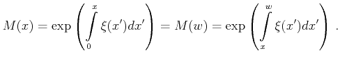
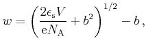
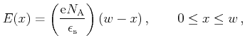
For an ideal BIB detector with no doping in the blocking layer a one dimensional Poisson equation can be formulated for the blocking and the depletion area, which gives the depletion width as [Szmulowicz87]
The electric field depends on the spatial coordinate ![]()
Another quantity of interest is the optical carrier generation rate ![]() . If
the reflectivity of the transparent contact is
. If
the reflectivity of the transparent contact is ![]() and the reflectivity of
the interface between the IR active layer and the substrate is
and the reflectivity of
the interface between the IR active layer and the substrate is ![]() ,
,
![]() can be written as [Szmulowicz80]
[Szmulowicz86]
can be written as [Szmulowicz80]
[Szmulowicz86]
In the depletion region the continuity equation for the electrons in the conduction band is
 |
(6.9) |
Equation (6.10) can be simplified if an ideal blocking layer is
assumed, which prevents the injection of hopping carriers so that
![]() . Furthermore, it can be assumed that the current density
. Furthermore, it can be assumed that the current density ![]() which stems from diffusion of carriers from the heavily doped neutral part of
the IR-active region is small enough to be neglected. This simplifies the
equation for the total current density to
which stems from diffusion of carriers from the heavily doped neutral part of
the IR-active region is small enough to be neglected. This simplifies the
equation for the total current density to
Semiconductors exhibit intrinsic conductivity at sufficiently high temperatures due to thermal activation of carriers from the valence band to the conduction band. A wide band gap causes a rapid decrease of this kind of conduction at lower temperatures. Therefore shallow impurities become the most important provider for free carriers as their ionization energy is much lower than the bandgap. At low temperatures the thermal activation energy is so small that the carriers are recaptured by the impurities. This is a gradual process known as freeze-out.
At even lower temperatures the impurities are completely frozen out and
hopping conduction is the prominent transport effect. In the
case of no compensation hopping conduction can occur - if an n-type
semiconductor is considered - when an electron is removed from a neutral donor
site and moves to a neighbor neutral donor site, creating an overcharged
impurity there [Nishimura65]. The conductivity ![]() caused by this
thermally activated process is characterized by an activation energy
caused by this
thermally activated process is characterized by an activation energy
![]()
 |
(6.15) |
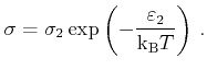
In n-type BIB devices the donor concentration is slightly compensated by a
frozen acceptor doping. The acceptors are ionized with carriers from the
impurity band, leaving positively charged donor sites in the impurity band even
at the lowest temperatures. Such a setup gives rise to another carrier hopping
effect, where the electron of a neutral donor site is transfered to a
positively charged neighbor donor site. This process is assisted by the
absorption and emission of a phonon, lifting the electron to an excited
intermediate state as illustrated in Figure 6.3 for a n-type device.
The conductance can be described with another thermal activation energy
![]() [Shklovskii84]
[Shklovskii84]
 |
(6.16) |
![\includegraphics[scale=0.75, clip]{inkscape_fig/hopping.eps}](img709.png)
|
A two step procedure is used to simulate the properties of BIB detectors. First the electrostatic field is calculated using a conventional TCAD device simulator. In this work MINIMOS-NT [IuE04] was used. This field is then fed to the Monte Carlo simulator where in a second step the Boltzmann equation is solved. The detector is modeled as a one-dimensional device.
The following sections show some features for Monte Carlo simulation at very low temperatures and present a concept for an alternative impact ionization model to capture a non-Markovian avalanche effect.
![\includegraphics[width=3.6in]{xmgrace-files/Neutral.eps}](img710.png)
|
At very low temperatures neutral impurity scattering can significantly contribute to the total scattering rate. In literature several attempts exists to describe neutral impurity scattering [Sclar56][Kwong90][Itoh97]. For the sake of simplicity the expression of Erginsoy [Erginsoy50][Bhattacharyya93] is used for the scattering probability
Figure 6.4 depicts the low field mobility of electrons in Si in the low temperature regime. Shown are MC simulation results based on phonon scattering and in addition neutral impurity scattering when indicated. It is shown that neutral impurities cause a mobility reduction at low temperatures, and therefore neutral impurity scattering has to be considered in simulation of BIB devices.
An BIB detector can also operate as a single photon multiplier if the bias voltage is large enough to cause an avalanche effect to due impact ionization. In the following, an impact ionization model is described which captures the non-Markovian nature of the avalanche [Sinitsa02][Petroff87].
It is assumed that impact ionization takes place exclusively in
the depletion region and that the carriers do not recombine again. The impact
ionization rate
![]() is derived from
(3.52), taking into account that the rate depends on the impurity
concentration
is derived from
(3.52), taking into account that the rate depends on the impurity
concentration
![]() of the impurity band
of the impurity band
| (6.18) |
Because of their low mobility the carriers in the impurity band experience no avalanche multiplication. As another consequence of the low mobility, the slow carriers in the impurity band cause a local breakdown of the field in the areas of avalanche generation [Petroff87]. This leads to a limitation of carrier multiplication. With Monte Carlo this effect can only be treated by applying a self-consistent simulation scheme.
|
![\includegraphics[width=3.7in]{bib-results/FieldCmp2.eps}](img723.png)
|
![\includegraphics[width=3.7in]{bib-results/dopingCmp2.eps}](img724.png)
|
These figures also illustrate some basic rules for the design of BIB
devices. It is shown how the depletion area is determined by the bias ![]() and
the compensation doping. To achieve good quantum efficency it is necessary to
have a large depletion area, because this is the part of the IR-active layer
where the field is non-zero and so the optical generated electrons are able to
proceed to the contact.
and
the compensation doping. To achieve good quantum efficency it is necessary to
have a large depletion area, because this is the part of the IR-active layer
where the field is non-zero and so the optical generated electrons are able to
proceed to the contact.
On the other hand, to avoid a breakdown condition, the depletion region must not grow into the contact. As a consequence the compensating acceptor doping must be well controlled at a quite low level.
It should also be noted that the field distribution does not depend on the majority doping, which forms the impurity band. In principle, a higher donor concentration leads to higher quantum efficency, but also introduces band broadening, which in turn leads to unwanted thermal dark current.
For the following simulations the field distribution is obtained by a conventional TCAD simulator and then passed to the Monte Carlo simulator, here VMC. Then a non-selfconsistent Monte Carlo simulation is performed.
When a photon is detected, it lifts an electron from the impurity band to the
conduction band, which - if the field is sufficiently large - causes
an avalanche multiplication. Two positions for the photon detection at
![]() µm
and
µm
and
![]() µm
are evaluated as depicted in Figure 6.7. Each
injection position is simulated 1000 times. In this setup the bias voltage
µm
are evaluated as depicted in Figure 6.7. Each
injection position is simulated 1000 times. In this setup the bias voltage
![]() and the acceptor doping concentration in the IR-active
region is
and the acceptor doping concentration in the IR-active
region is
![]() . All other device
specifications are in accordance with Table 6.1.
. All other device
specifications are in accordance with Table 6.1.
Figure 6.9 depicts the energy distribution of electrons collected
at the contact for an assumed optical generation of the original electron at
position ![]() . The mean energy is 46.4meV which is only slightly below the
energy of electrons starting at position
. The mean energy is 46.4meV which is only slightly below the
energy of electrons starting at position ![]() . This indicates that the impact
ionization limits the energy gain of the carriers as they proceed through the
depletion region.
. This indicates that the impact
ionization limits the energy gain of the carriers as they proceed through the
depletion region.
Figure 6.10 and Figure 6.11 show the shape of the electron avalanche, when
it reaches the contact, for electrons generated at position ![]() and
and ![]() respectively.
respectively.
It should be noted that these results are not calibrated against measurement data and therefore only give qualitative insights about the avalanche behavior.
![\includegraphics[width=3.7in]{bib-results/pos2500.eps}](img729.png)
|
![\includegraphics[scale=0.65, clip]{inkscape/device11.eps}](img660.png)
![\includegraphics[scale=0.65, clip]{inkscape/band10.eps}](img661.png)

![$\displaystyle M(x)=\exp\left[N_{\mathrm{D}} \sigma_{\mathrm{I}} \left(we^{- \fr...
...e^{-t}}{t}dt + A \int_{\frac{A}{w-x}}^\infty \frac{e^{-t}}{t}dt \right) \right]$](img703.png)


![\includegraphics[width=3.7in]{bib-results/energyDist10.eps}](img730.png)
![\includegraphics[width=3.7in]{bib-results/energyDist14.eps}](img731.png)
![\includegraphics[width=3.7in]{bib-results/timeDist10.eps}](img732.png)
![\includegraphics[width=3.7in]{bib-results/timeDist14.eps}](img733.png)