Previous: Acknowledgment Up: Dissertation Robert Klima Next: 1.1 History of Three-Dimensional Device Simulation
The electronics industry has grown rapidly within the last three decades driven by the revolution in microelectronics. Nowadays, complex circuits containing millions of transistors acting as switches are combined on a single chip. Processors and electronic circuits are built for a multitude of different applications and can be found in almost every electrical device.
The first description of an insulated-gate-field-effect transistor (IGFET) can be found in the historical patent of Lilienfield [1] dating from 1926. It depicts a device containing three contacts, where a current flow between two of them is controlled by a vertical field. The vertical field is applied by a voltage to the third contact which is dielectrically insulated from the rest of the device. Unfortunately the technology at that time was unable to produce the device. With the invention of the bipolar transistor in 1947 [2] and its enormous success IGFET technology was completely overshadowed and forgotten for a while.
Many years later, the technology reached a level of maturity which was sufficient to produce good quality gate oxides. In 1960, Kahng and Atalla [3] developed the first working MOSFET evolved from the IGFET of Lilienfield. In the early 1960s, putting just a few transistors on one single chip was considered cutting edge. Advancements in monolithic integrated circuits increased the important role of the MOSFET technology and CMOS technology is still the driving technology in the microelectronic industry.
In 1958, Jack S. Kilby conceived and built the first electronic circuit in which all of the components both active and passive, were fabricated on a single piece of semiconductor material. For this effort he was honored with the 2000 Nobel price in physics. In 1965, just a few years after the first planar integrated circuit was fabricated, Gordon Moore made his famous observation which is known today as ``Moore's Law'' [4]. In his original paper [5] Moore predicted that the number of transistors per integrated circuit would double every year. Unlike a forecast the industry tried to meet his prediction. In 1975 Moore updated his prognosis that the number of transistors will double every second year [6] and and it still holds true in the first decade of the new millennium.
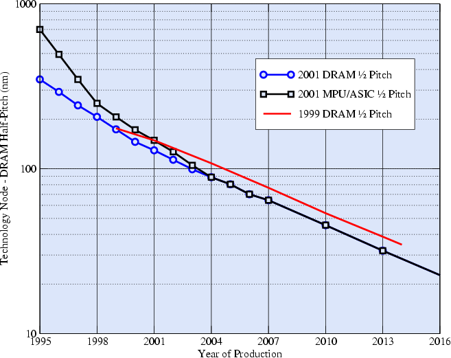
In 1992 the Semiconductor Industry Association (SIA) published the ``National Technology Roadmap for Semiconductors (NTRS)'' which provided a 15-year outlook on the major trends of the semiconductor industry. The roadmap contained requirements and possible solutions and was updated in 1994 and 1997. The NTRS was a good reference document for semiconductor manufacturers, included forecasts on materials and software, and provided clear targets for researchers in the following years. In 1998 NTRS was replaced by the ``International Technology Roadmap for Semiconductors (ITRS)'' to benefit from inputs from all over the world. Since 1998 ITRS was issued or updated annually. Fig. 1.1 shows the forecast for the DRAM interconnect half-pitch nodes for the period of 2001 to 2016 taken from the ITRS 2001 [7].
While basic discoveries and inventions between 1945 and 1970 laid the foundations for semiconductor technology, in the past 30 years chip complexity increased exponentially. The reason for this accelerated growth is primarily due to the constant reduction of the device geometries, improved technologies, and new inventions which enable the implementation of special functions in new ways and in smaller areas. The shrinkage of the geometries allows more devices to be placed on a chip. Improved technologies permit larger chips to be fabricated more economically with lower drop out ratios and enable new device structures. It is widely expected that these historical trends will continue for the next 10 to 20 years resulting in chips containing billions of transistors.
Semiconductor technology has evolved mainly by means of empirical methods. The progress of technology is so fast, that the scientific understanding of those technologies is inadequate to fully grasp or predict the behavior of a device exactly. Nevertheless, device simulation turned out to be the only way to study the electrical behavior inside the device. It enables investigations of physical quantities like potential distribution and current transport which cannot be obtained by practical measurements. The very first simulators only solved Poisson's equation and one carrier continuity equation in steady state for one-dimensional structures using many simplifications of models and physical effects due to the limited computational power.
More reliable simulation tools led to dramatic changes of the semiconductor technology. Errors compared to measurements are mainly due to modeling errors, e.g., simplification of relevant equations, simplifications of device geometries, material properties and doping profiles which cannot be measured exactly, and physical effects which are not taken into account or are a priori not known. Within the last three decades, device simulation became an important tool for understanding the behavior of semiconductor devices.
With the increased performance and memory of computers, two-dimensional simulators have been developed enabling a more realistic description of the geometries and the structure of the devices. Sophisticated numerical algorithms and solvers have been developed to reduce the computational burden of the simulations. Two continuity equations (one for electrons and one for holes) have been applied replacing the inaccurate approximation of the carrier equation used before. Much effort was put on the development and implementation of more realistic models which account for the most important physical effects. This supported the dramatic innovation of semiconductor technology and the dramatic miniaturization process which again had a strong influence on the development and the capabilities of the simulation tools.
With the increased integration density of integrated circuits the feature sizes
of the devices become smaller and smaller. Nowadays, MOS device structures with
gate lengths below
![]() and gate oxide thicknesses below
and gate oxide thicknesses below
![]() are state-of-the-art. Due to miniaturization, three-dimensional
effects become more pronounced, and the three-dimensional device geometries
noticeably influence the electrical characteristics of the devices. Therefore,
three-dimensional device simulations have to be performed.
are state-of-the-art. Due to miniaturization, three-dimensional
effects become more pronounced, and the three-dimensional device geometries
noticeably influence the electrical characteristics of the devices. Therefore,
three-dimensional device simulations have to be performed.
The first device which unveiled its three-dimensional shape was the Dynamic Random Access Memory (DRAM) Cell where the capacitor holding the charge was realized by a trench etched into the bulk of the semiconductor [8]. Before, DRAM cells used a planar MOS-capacitor at the surface to store the charge. For leakage current investigations three-dimensional simulation became mandatory. Another well known example are three-dimensional effects in MOSFETs when the width of the channel becomes comparable to its length. A couple of publications [9,10,11,12,13,14,15,16,17] focus on this effect which is called ``narrow channel effect''. For all these examples two-dimensional simulations cannot predict the device behavior. Instead three-dimensional simulations have to be performed to fully describe the device.