Previous: 4.2 MagFET Up: 4.2 MagFET Next: 4.2.2 Results
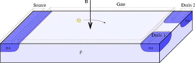
Fig. 4.8 shows the structure of a MAGFET. The printed gate
length is
![]() , the oxide thickness is
, the oxide thickness is
![]() and
the device width is
and
the device width is
![]() . The drain is split into two contacts
with a distance of
. The drain is split into two contacts
with a distance of
![]() from each other. If no magnetic field
is applied and the bias polarization at the drains are the same, the device
behaves exactly like a MOSFET. However, if a magnetic field is present
(
from each other. If no magnetic field
is applied and the bias polarization at the drains are the same, the device
behaves exactly like a MOSFET. However, if a magnetic field is present
(
![]() ) the carriers in the channel are deflected as a result of the
Lorentz force
) the carriers in the channel are deflected as a result of the
Lorentz force
where
![]() denotes the Lorentz force,
denotes the Lorentz force, ![]() is the charge of the carriers,
and
is the charge of the carriers,
and
![]() is the carrier velocity. This charge deflection results in a
perturbed balance of the current flow in the channel area and thus in different
currents
is the carrier velocity. This charge deflection results in a
perturbed balance of the current flow in the channel area and thus in different
currents
![]() and
and
![]() measured in the two drains.
measured in the two drains. ![]() is a function of
is a function of
![]() and the geometry of the device [145]. The relative
sensitivity
and the geometry of the device [145]. The relative
sensitivity ![]()
![]() %
%![]() of a MAGFET is defined as
of a MAGFET is defined as
where ![]() denotes the total current
denotes the total current
![]() . In
[147] the sensitivity is obtained as a function of several geometric
parameters, such as the distance of the two drains, the channel length, the
width of the source contact, and the gate overlap, but also the gate and the
drain voltages. Moreover, the sensitivity is dramatically increased for low
temperatures [K7].
. In
[147] the sensitivity is obtained as a function of several geometric
parameters, such as the distance of the two drains, the channel length, the
width of the source contact, and the gate overlap, but also the gate and the
drain voltages. Moreover, the sensitivity is dramatically increased for low
temperatures [K7].
Robert Klima 2003-02-06