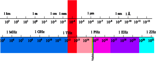
Figure 2.1: The terahertz spectrum is located between the optical domain
and the microwave domain.
For more than 35 years, semiconductor nanostructures have been investigated for a large number of applications in technology including lasers, photodetectors, light emitting diodes, and transistors. Nowadays, these structures are considered to be even more perspective for novel applications. This is why after such a long period the intensive research performed in this field even grows further.
If the geometrical extent of a semiconductor, typically embedded in the matrix of another semiconductor, is reduced in one, two or three directions of space below the size of the ”de Broglie wavelength” of a charge carrier which is on the order of a few nanometers, it is called a nanostructure [1].
The electrical and optical properties of low-dimensional structures, including their interactions such as electron-electron, electron-hole, and electron-photon interaction, depend qualitatively on the dimensionality of the structure and quantitatively on details of the geometry of the structure such as size and shape, and on the distribution of the atoms inside [1]. The electronic properties in turn control the linear and nonlinear optical and electronic transport properties. Thus ”geometrical architecture” opens enormous opportunities for designing completely novel materials or heterostructures.
The far-infrared (FIR) frequency range is roughly defined as 30-300 μm or 4-40 meV and is often referred to as the terahertz frequency range 1-10 THz [2–4], see Fig. 2.1. FIR electromagnetic radiation is important in many applications such as radio astronomy, environmental monitoring, plasmon diagnostics, laboratory spectroscopy, telecommunications, medicine etc. and in the characterization of nanoscale condensed matter materials. In recent years, the generation, propagation and detection of FIR electromagnetic radiation using two-dimensional semiconductor systems or other semiconductor nanostructures has become one of the most rapidly expanding fields in photonics, optoelectronics and condensed matter physics.
However, the terahertz frequency range cannot be directly accessed. Diode lasers are ideal sources because they are cheap, compact and very efficient. However, the semiconductor bandgap places a limitation on emission frequency. The longest-wavelength diode lasers (~ 30μm) are based on narrow gap lead-salt semiconductors [5]. While these lead-salt lasers have been quite successful for high resolution spectroscopy, they are still limited to cryogenic operation and provide relatively low power. On the other end of the spectrum, semiconductor transistors can be used to generate 100 GHz oscillators [6]. Molecular gas lasers are one of the practical laser sources for the FIR, but they have limited lasing frequencies. They are also somewhat unwieldy as they require high voltage supplies and are usually rather bulky.
Semiconductor nanostructures are most promising candidates to solve the lack of suitable sources and detectors in the FIR frequency range. Graphene nanostructures [7–12] and quantum cascade devices [13–22] promise efficient operation in a broad frequency range. Electronically, pure graphene is a gapless semiconductor. Since the potential usefulness of graphene in electronic and photonic applications cannot be fully tapped unless a bandgap can be engineered, bandgap engineering of graphene has attracted much research interest recently. In gapped graphene, a vertical linear response peak is predicted when the photon frequency matches the bandgap energy. Stripped into a few nanometer-wide graphene nanoribbon, the bandgap can be tuned to a certain extent by the confinement of electronic wave function. One dimensional graphene nanoribbons and superlattices provide precise tunable energy gaps for optical applications.
Bandgap engineering of graphene-based structures could result in devices operating in the terahertz domain. Bandgap engineering for terahertz operation is also possible in intersubband quantum cascade heterostructures [23]. Intersubband optical devices have several advantages over conventional interband semiconductor devices. Most useful is the fact that the emission frequency is determined by the design of the heterostructure and can hence be tailored to the application. This is especially useful for infrared applications where small bandgap materials become difficult to find and work with. Also, since the envelope functions extend over a well (tens of Angstroms), the dipole moment for the intersubband transition is typically several orders of magnitude larger than that of an atomic transition.