|
|
|
|
Dissertation Christian Poschalko | |
| Previous: 3.2 Direct radiation from a PCB which is Up: 3 Electromagnetic emissions mechanisms from PCBs Next: 4 Cavity model of the electromagnetic field between | ||||
|
|
|
|
Dissertation Christian Poschalko | |
| Previous: 3.2 Direct radiation from a PCB which is Up: 3 Electromagnetic emissions mechanisms from PCBs Next: 4 Cavity model of the electromagnetic field between | ||||
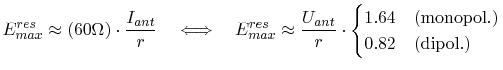
Generally all emission mechanisms in this section are common impedance coupling mechanisms. Figure 3.3 illustrates the common impedance coupling mechanisms of a source circuit to a victim circuit. A common resistor Rk couples the two circuits in Figure 3.3(a) galvanically. The coupling capacitance Ck in Figure 3.3(b) couples a noise voltage to a victim circuit. Inductive coupling of a source loop and a victim loop is depicted in Figure 3.3(c). The right circuit diagram in Figure 3.3(c) is equivalent to the left diagram. It illustrates the possibility to consider the inductive coupling with a coupling inductance Lk. The victim circuit in Figure 3.3 is a sensitive sensor circuit and the measurement of the sensor voltage is denoted by Uk. However, the victim circuit may also be any other circuit on the PCB. Extended circuits on the PCB, circuits with attached cables, or sizeable daughter boards are the unintentional emission antennas which are supplied from the coupled currents and voltages. When the antenna of the victim circuit is located far away from the coupling fields, the whole coupled field will not change significantly, even when the antenna is replaced by a different one. Therefore, the coupling impedances enable the description of the source coupling to an antenna, independent of the antenna. This provides the opportunity to classify the PCB structures regarding their emissions relevance with only the coupling impedances and without considering the antenna structure. For example, the consideration of a cable attached to a PCB in an emission simulation will also show the cable resonances. However, when this cable cannot be modified by the PCB designer and, especially, when the PCB should be connected to different cables in different applications, a simulation result including these resonances is misleading. The PCB emission optimization can be performed more efficiently by omitting the cable, just by simulating the coupling impedances. A separate simulation of the antenna can be used for quantitative prediction simulations. According to [62], the maximum radiated far field from cables can be estimated roughly with a simple line resonator model. The estimated maximum electric fields from monopol and dipole antennas at their resonance are [62]
![\includegraphics[height=4.9 cm,viewport=70 600 295
760,clip]{pics/Coupling.eps}](img225.png)
![\includegraphics[height=5 cm,viewport=300 600 570
760,clip]{pics/Coupling.eps}](img226.png)
| (a) Galvanic coupling. | (b) Capacitive Coupling. |
![\includegraphics[height=5 cm,viewport=70 420 570
590,clip]{pics/Coupling.eps}](img227.png)
| (c) Inductive Coupling. |
In the following an example for common impedance coupling in a power delivery network is presented. Every real power supply has a nonzero impedance. Thus, currents from one device cause a voltage noise on that impedance, which is conducted to other devices connected to the same power supply. An example is an automotive control device connected to the board power net which also supplies many other electronic devices. Another example is a three-phase converter for an electric drive, supplied from a transformer station which might supply a whole village. Figure 3.4 depicts a push-pull switching stage, supplied from a battery, which also supplies a sensitive sensor circuit. Power supply noise generated from the switching circuit couples to the sensitive circuit through a non zero resistive impedance of the power supply R1 and an inductive coupling of the loops considered with a coupling factor K1 which partly couples the inductance of the source path L3 and the inductance of the victim path L6. As an alternative to the coupling factor, one could also consider the inductive coupling with an inductance in series to the resistor R1.
![\includegraphics[height=8.7 cm,viewport=70 500 540 760,clip]{pics/CE_Example.eps}](img228.png) |
![\includegraphics[height=10 cm,viewport=50 470 520 780,clip]{pics/CE_FFT.eps}](img229.png) |
The next part contains the development of a cavity model for the efficient simulation of the emissions from a printed circuit board under a metallic enclosure cover. The model enables the explicit calculation of the common mode coupling impedances from printed circuit board structures to the interface at the apertures of the enclosure. This provides the opportunity to optimize the interior of the device independent of the external environment.
C. Poschalko: The Simulation of Emission from Printed Circuit Boards under a Metallic Cover