


Next: 8.1.1 Modeling the Fabrication
Up: 8. Technology Optimization
Previous: 8. Technology Optimization
A common problem with MOS devices is their degradation in the presence
of hot carriers in their channels [14,25]. These hot
carriers are critical to the lifetime of a MOS device since they are
-- due to their high energy -- able to penetrate the gate oxide film
and degrade the function of the device. As an effect of trapped
gate-oxide charges, the threshold voltage is increasingly shifted with
time and at some point the integrated circuit fails. At the same time
hot carriers are the cause for electron/hole pair generation by means
of impact ionization mechanisms [43]. Pair generation
gives rise to the substrate current of the devices and, since they are
correlated to hot carriers, they serve as a macroscopic measure for
the extent of hot carriers. This means by reducing the substrate
current of a MOS device, hot carrier effects are reduced
simultaneously.
The introduction of a lightly doped drain (LDD) structures reduces the
electric field at the drain end of the channel, and, thus, also
reduces hot carrier effects. On the other hand, a LDD also reduces the
drive current of the device due to an additional serial
resistance. This means that a compromise between reduced hot carrier
effects (or substrate currents) and a moderate reduction of the drive
current has to be found. Therefore, an optimization (minimization) of
the substrate current is expected to deliver MOS devices with
increased lifetime and an acceptable drive current.
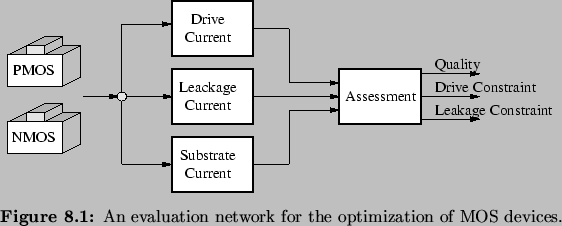
Figure 8.1 depicts the network which describes these
criteria. MOS devices are fabricated according to the parameters of a
process recipe and the set of lithography masks. Afterwards, the drive
current, the maximum substrate current, and the leakage current of
that device are evaluated. And finally, a quality metric (which is used
as the target of the optimization8.1) is computed based on the evaluated substrate current
according to
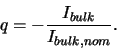 |
(8.1) |
In order to force the optimization not to reduce the drive current
Ion we use an inequality constraint
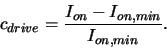 |
(8.2) |
As a result the optimizer has to maintain the drive current above a
lower limit
Ion,min= 0.24 mA.
Similar to the drive current, we include another constraint for the
leakage current in order to avoid devices which are susceptible to
punch through breakdown. We therefore specify an upper limit of
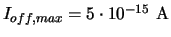 and compute the constraint
according to
and compute the constraint
according to
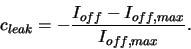 |
(8.3) |
Fußnoten
- ... optimization8.1
- Since the DONOPT
optimizer minimizes its target, we design a quality metric with
negative sign.
Next: 8.1.1 Modeling the Fabrication
Up: 8. Technology Optimization
Previous: 8. Technology Optimization
Rudi Strasser
1999-05-27