On the high-performance end of the technology spectrum power
consumption will be limited by the maximum allowable thermal
dissipation.
The 1997 SIA roadmap [4] projects a maximum power of 175W
(with heat sink) at
![]() for the year 20E.
This would mean a supply current in the range of 300A.
From the viewpoint of characteristic impedance this means
a value of
for the year 20E.
This would mean a supply current in the range of 300A.
From the viewpoint of characteristic impedance this means
a value of
![]() which is
more than five orders of magnitude away from
the free-space characteristic impedance of
which is
more than five orders of magnitude away from
the free-space characteristic impedance of ![]() .
2.4
The main challenge is to deliver
large amounts of power at
very low voltages
economically.
The most likely solution is the combination of
.
2.4
The main challenge is to deliver
large amounts of power at
very low voltages
economically.
The most likely solution is the combination of
The design of converter circuits for very low voltages is not a straight-forward task, albeit not impossible. Because of their high forward voltage the diodes which are usually used as passive switches must be replaced by MOSFETs, and because normal pn-junction diodes would inject minority carriers into the wells and substrate, resulting in excess leakage and low switching speed. Energy storage components used in on-chip converter circuits (capacitors, inductors) can be kept small because the converters can run at very high frequencies when implemented in a high-performance ULP technology. Table 2.7 compares the key elements of conventional and low-voltage converters.
| element | conventional | low-voltage |
| active switch | MOSFET, BJT | fast MOSFET |
| passive switch | diode | fast MOSFET |
| energy storage | capacitance, inductance | small capacitance, small inductance |
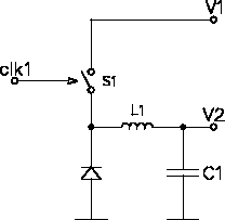
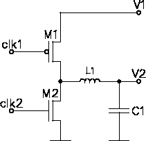
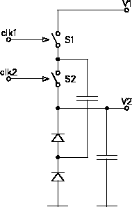
One well-known converter principle is the switched-capacitor (SC) converter. The low-voltage is shown in Fig. 2.14. It can be regarded as a voltage divider or doubler (operating in reverse direction). The clocking signals clk1 and clk2 can be generated as shown in Fig. 2.15. When a clock signal is applied to the input A the rising edge of X1 occurs T after that of X2, and the falling edge of X2 occurs T after that of X1, eliminating the crowbar current through the transistors. clk3 and clk4 are level shifted versions of clk1 and clk2 respectively. The advantages of this SC converter circuit are that it needs only capacitors for energy storage and each transistor ``sees'' at most the output voltage across its terminals. The main drawback is that the current flows across two switches instead of one and the requirement of a fairly large floating capacitor.
Note, that this converter in its low-voltage form
works bidirectionally. It is usually not an objective to up-convert
the internal supply voltage. However, this feature can be used
effectively to operate two low-voltage loads in series and have the
converter provide the balancing current. The remaining problem
is that in the upper load circuit the NMOS transistors see a higher
![]() and therefore have a reduced on-state current. This could be eliminated by
employing a triple-well technology or MCM. Also, in a deep-sub-micron
technology the body effect is less pronounced.
and therefore have a reduced on-state current. This could be eliminated by
employing a triple-well technology or MCM. Also, in a deep-sub-micron
technology the body effect is less pronounced.
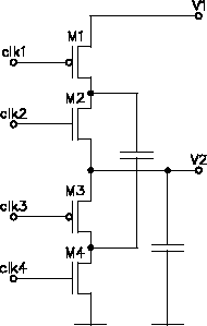
Another well-known converter is the buck (or fly-back) converter shown in Fig. 2.16. The voltage ratio V1/V2 is determined by the duty cycle factor of the switch control signal clk1, ranging from 0 to 1. The main advantage of the buck converter is its flexibility and simplicity. A drawback is the use of an inductance for energy storage. This inductance, however, can be very simple (in some cases some bonding wire may be sufficient). The control circuit (see Fig. 2.15) to generate the signals clk1 and clk2 may be tuned to support adiabatic charging and discharging of the transistors' output capacitances. As in the case of the SC converter, the low-voltage version of the buck converter works bidirectionally.
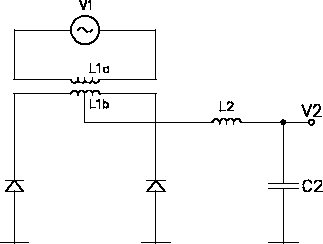
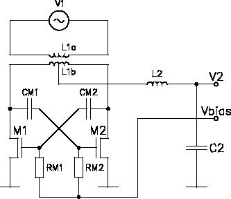
The simplest way to build a mains power supply is to take a transformer with a center-tapped secondary winding, two rectifier diodes, and a capacitor with an optional smoothing inductance. The low-voltage version of this principle is shown in Fig. 2.17. The input of this circuit is a high-frequency AC voltage, which is down-converted by the transformer L1a/L1b, and then rectified by M1/M2 and smoothed by L2/C2. The advantage of this circuit is that it supports AC powering and it uses only NMOS transistors. The disadvantage is the need for an additional transformer and the transistors must withstand 2 V2.
Note, that this circuit works bidirectionally as well: when a DC voltage is applied to the output L1b then M1, and M2 will oscillate. This can cause a general instability of the rectifier, if badly designed. On the other hand, this operation mode can also be used for transmitters, e.g., in remote-sensing applications.
![\includegraphics[scale=0.9]{invdrv.ps}](img342.gif)