Key issues of the deposition processes are the geometry, modeling of the source, collision in transit from the source to the feature, and the collision and sticking rate of the material being deposited.
In this chapter we present simulation results for the backend of a 100
![]() process, where the influence of void formation between metal lines
profoundly impacts the performance of the whole interconnect stack
consisting of aluminum metal lines and titanium nitride local
interconnects. Feature-scale topography simulations serve here as input to subsequent
capacitance extraction. The entirety of simulations and extracted
capacitances characterize a specific technology and are made
accessible to the circuit designer via a database.
process, where the influence of void formation between metal lines
profoundly impacts the performance of the whole interconnect stack
consisting of aluminum metal lines and titanium nitride local
interconnects. Feature-scale topography simulations serve here as input to subsequent
capacitance extraction. The entirety of simulations and extracted
capacitances characterize a specific technology and are made
accessible to the circuit designer via a database.
One of the challenges that TCAD must currently meet is the analysis of the performance of groups of components, interconnects, and - generally speaking - large parts of the IC. This enables predictions that the simulation of single components cannot achieve. In this chapter we focus on the simulation of backend processes, interconnect capacitances, and time delays. The simulation flows start from the blank wafer surface and the final result is device information for the circuit designer using circuit simulators such as SPICE (simulation program with integrated circuit emphasis)6.1.
Interconnects are becoming increasingly important as the shrinking of the semiconductor technologies continues, since the timing delays due to metal lines contribute increasingly to the overall delay. Therefore, it is imperative for predictive TCAD applications that capacitance and resistance of interconnect lines are modeled as accurately as possible.
Most RCX (resistance and capacitance extraction) tools assume rectangular metal profiles, either planar or conformal dielectrics, and they use simplistic void models. Even if the metal slope is modeled, it is mostly assumed constant and independent of space. While these idealizing assumptions may be sufficient for past technologies, they are insufficient for today's technologies like the 100nm process considered in Section 6.4, where interconnects show a number of special features which are nowhere close to ideal.
For proper modeling of the capacitance, one has to know the metal profile, e.g., bottom and top CD s (critical dimension) and metal slope, the profile of the deposited layer with and without CMP, and the profile of the void, if it forms. Generally these three profiles depend heavily on the conditions of the deposition process, on metal thickness and line-to-line spacing, and to a lesser degree on the metal width [8,10].
In order to join topography and backend simulations, deposition, etching, and CMP processes in the various metal lines are used to build up the backend stack starting from the flat wafer surface. Depending on the metal combination, line-to-line spacing, and line width, thousands of simulations are required whose results are stored in a database.
![\includegraphics[width=0.7\linewidth]{figures-capacitance-journal/figures/mod2740-4-cropped}](img356.png)
|
Having described the handling of moving boundaries in Chapter 5, this section focuses on the chemical surface reactions. Starting from a plain substrate, the principal topography simulation steps are etching trenches, depositing thin films, and CMP (cf. Figure 6.1). Finally we outline how the single topography simulations are integrated to yield larger backend structures.
In the considered backend process the deposited films are silicon nitride and silicon dioxide films (cf. Section 6.4). Here the transport of particles happens in the radiosity regime and the deposition processes are governed by luminescent reflection.
The silicon nitride films were deposited by PECVD (plasma enhanced CVD) from silane and
NH![]() and were not doped. The chemical reaction is
and were not doped. The chemical reaction is
![]() [74]. For simulation
purposes this was considered as the essential reaction,
a detailed model including triaminosilane condensation can be found in
[94]. The silicon dioxide film is deposited from a TEOS process which has
been treated in Chapter 4.
[74]. For simulation
purposes this was considered as the essential reaction,
a detailed model including triaminosilane condensation can be found in
[94]. The silicon dioxide film is deposited from a TEOS process which has
been treated in Chapter 4.
In order to calculate the thickness
![]() of the film deposited during a time interval of length
of the film deposited during a time interval of length
![]() , we observe that
, we observe that ![]() is proportional to
is proportional to ![]() ,
to an Arrhenius term, and to the deposition rate
,
to an Arrhenius term, and to the deposition rate ![]() corresponding to
the chosen deposition model. This implies
corresponding to
the chosen deposition model. This implies
![]() . Here
. Here
![]() is the Arrhenius term
with activation energy
is the Arrhenius term
with activation energy ![]() , absolute temperature
, absolute temperature ![]() , a
pre-exponential constant
, a
pre-exponential constant ![]() , and
, and ![]() is the deposition rate
[67].
is the deposition rate
[67].
When modeling topography processes it is generally possible to write down complicated reaction paths and list dozens of possible surface reactions. However, it is not straightforward to determine the vital reactions and their constants. Thus it is important to reduce the possible reaction paths to an essential minimum (cf. Chapter 4).
Figure 6.2 shows the simulation result for the process mentioned above which has been used for the calculation of capacitance.
On the feature-scale level the simulation of CMP can be performed in a straightforward manner, since the thickness of the remaining part of the layer is known. In this simulation step the boundary is modified so that all parts above the given thickness are removed and the remaining points are joined accordingly.
![\includegraphics[width=0.9\linewidth]{figures-capacitance-journal/figures-2/0-45}](img368.png)
|
![\includegraphics[width=0.9\linewidth]{figures-capacitance-journal/figures-2/0-90}](img370.png)
|
![\includegraphics[width=0.9\linewidth]{figures-capacitance-journal/figures-2/1-50}](img372.png)
|
![\includegraphics[width=0.82\linewidth]{figures-capacitance-journal/figures/skeleton}](img373.png)
|
Simulations of single features, performed by the above steps, can be
duplicated using affine transformations
![]() to obtain more complex structures. For example, to arrive at the structures shown in
Figures 6.3, 6.4,
and 6.5, it
is necessary to simulate the processes for a single feature including
etching and subsequent deposition. The resulting boundaries are
duplicated by affine transformations. At the left and right
boundaries, other simulations have to be performed, as they are
formed by half trenches. The results for the left hand boundary are
mirrored to yield the right hand boundary.
to obtain more complex structures. For example, to arrive at the structures shown in
Figures 6.3, 6.4,
and 6.5, it
is necessary to simulate the processes for a single feature including
etching and subsequent deposition. The resulting boundaries are
duplicated by affine transformations. At the left and right
boundaries, other simulations have to be performed, as they are
formed by half trenches. The results for the left hand boundary are
mirrored to yield the right hand boundary.
The coordinates of the structures simulated by topography simulator serve as input to calculate the electric filed. For the following simulations RAPHAEL [7] was used. RAPHAEL is a solver for electrical field and calculates the charge densities and various capacitances. Depending on the required resolution, the simulator yields a large number of points describing ILD (interlevel dielectrics) and voids. Since this number of surface elements determines the number of RAPHAEL grid points and simulation time is an important factor, a significant reduction of the number of points is necessary. Otherwise simulation times would be orders of magnitude larger than those of equivalent simplified structures. Hence we use a surface-coarsening algorithm to rework the output and to reduce the number of points supplied to the RAPHAEL [36].
For example one can assume that a signal line is at
high voltage and surrounded by two lines on the left, two lines on the
right, a plane underneath, and, if necessary, a plane above. The
surrounding lines and planes are assumed to be grounded. For
example an M![]() signal line could be surrounded by M
signal line could be surrounded by M![]() grounded lines
above the M
grounded lines
above the M![]() plane and underneath the M
plane and underneath the M![]() plane. This skeleton is
shown in Figure 6.6.
plane. This skeleton is
shown in Figure 6.6.
The second variable is line-to-line spacing. Simulations start from the
minimum allowed line-to-line spacing (e.g.,
![]() ) and end in the range
of a few microns (e.g.,
) and end in the range
of a few microns (e.g.,
![]() ). Generally, initial
line-to-line spacing
increments are fine to capture the strong dependence of the capacitance on
line-to-line spacing, while the final increments are coarse to capture capacitance
saturation.
). Generally, initial
line-to-line spacing
increments are fine to capture the strong dependence of the capacitance on
line-to-line spacing, while the final increments are coarse to capture capacitance
saturation.
Third, capacitance simulations depend on the line width. Simulations start from the minimum allowed width to approximately 60 times the minimum width. Since the dependence on width is well behaved, only a few intermediate widths are usually needed.
In order to verify ELSA, different interconnect and metal lines
structures provided by our industry partner have been considered to be
simulated. As an example, we consider the case of M![]() lines above the M
lines above the M![]() plane. These backend
stacks are part of a 100nm Aluminum/TEOS process (cf. the SEM image
shown in Figure 6.1). The films deposited are
silicon nitride and silicon dioxide films and the interconnect lines
are made of aluminum. The experiments performed during the development of
a RAM process were performed in a LAM 9600 reactor [12].
plane. These backend
stacks are part of a 100nm Aluminum/TEOS process (cf. the SEM image
shown in Figure 6.1). The films deposited are
silicon nitride and silicon dioxide films and the interconnect lines
are made of aluminum. The experiments performed during the development of
a RAM process were performed in a LAM 9600 reactor [12].
The M![]() lines have a width of
lines have a width of
![]() , and a line-to-line
spacing varying between
, and a line-to-line
spacing varying between
![]() and
and
![]() . Figure 6.3 shows the RAPHAEL
structure constructed from ELSA coordinates at minimum line-to-line spacing. Note
that at a minimum line-to-line spacing the metal lines are vertical
and voids have their maximum size. For a line-to-line spacing of
. Figure 6.3 shows the RAPHAEL
structure constructed from ELSA coordinates at minimum line-to-line spacing. Note
that at a minimum line-to-line spacing the metal lines are vertical
and voids have their maximum size. For a line-to-line spacing of
![]() , as shown in Figure 6.4, the side walls
are sloped and the voids are considerably smaller.
, as shown in Figure 6.4, the side walls
are sloped and the voids are considerably smaller.
Next we build the structure with a line-to-line spacing of
![]() .
Figure 6.5 shows the corresponding RAPHAEL
structure, again constructed from simulation results. Note
that in this case, however, the metal lines have a larger slope, which
duplicates the real process geometry. Voids are quite small in this
case. At
.
Figure 6.5 shows the corresponding RAPHAEL
structure, again constructed from simulation results. Note
that in this case, however, the metal lines have a larger slope, which
duplicates the real process geometry. Voids are quite small in this
case. At
![]() line-to-line spacing the metal slope has saturated and no
voids are formed.
line-to-line spacing the metal slope has saturated and no
voids are formed.
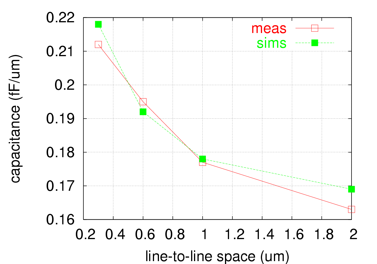
![\includegraphics[height=0.72\linewidth,angle=0]{figures-capacitance-journal/figures-2/capacitance}](img381.png)
|
|
The capacitance of the middle line was simulated for the above structures and compared to CBCM s (charge based capacitance measurement)6.2. The simulation results and measurements are compared in Figure 6.7. Simulation results show very good agreement with data obtained from measurements with a maximum error below 4%.
As a second example, we compare the capacitances extracted after
silicon dioxide deposition in the M![]() plane to CBCM s. Simulations
were performed for line-to-line spacings of
plane to CBCM s. Simulations
were performed for line-to-line spacings of
![]() ,
,
![]() ,
,
![]() , and
, and
![]() . The simulated and measured capacitances are shown in
Figure 6.8 and again the error is below 4%.
. The simulated and measured capacitances are shown in
Figure 6.8 and again the error is below 4%.
The two-dimensional models for lines surrounded by
other lines, as shown by these examples, are important since there is an abundance of cases where
they appear on a chip. One of the most important cases is the last
layer of the metal lines which are used as paths from one side of the chip to the
other. Such an example is a TCO (total cost of ownership) path whose length is
![]() in a 72Mbit DRAM chip which is
in a 72Mbit DRAM chip which is
![]() in
length. The TCO path is divided into eight portions, each portion
has a different width and different spacing to adjacent lines. It is
very important that this path is modeled accurately and optimized, as
it is used to fabricate products working at high operation
frequency. To predict and optimize the performance of this line,
very accurate models are needed motivating these simulations.
in
length. The TCO path is divided into eight portions, each portion
has a different width and different spacing to adjacent lines. It is
very important that this path is modeled accurately and optimized, as
it is used to fabricate products working at high operation
frequency. To predict and optimize the performance of this line,
very accurate models are needed motivating these simulations.
![\includegraphics[width=0.8\linewidth,bb=63 72 706 576]{figures/void-different-steps}](img388.png)
|
![\includegraphics[width=0.8\linewidth]{figures/void-different-scales2}](img390.png)
|
This difference originates from the extension of the speed function. Practically once a void forms, there is no more visibility between the void and source of deposition and the void and the deposited boundary, as well. Therefore, it is expected that the void is no longer displaced. However, depending on the width of the narrow band and the duration of a time step some points of the void do not leave the narrow band for a few simulation cycles and their adjacent grid points are assigned a non zero speed value during the extension of the speed function. This continues until the void is no longer inside the narrow band and leads to the change of shape of the void compared to its shape just after its formation.
As can be seen clearly in Figure 6.10, the form of the void extracted at the final step of the simulation is unrealistic since it contains steps which are not seen in the measurements. In addition, by extracting the void immediately after its formation, redundant points along vertical segments are eliminated and the subsequent coarsening is no longer required. However, the difference between the shapes does not influence the accuracy of the capacitance calculations and demands only additional simulation time due to the coarsening algorithms.
The immediate advantage of knowledge obtained from this study was a high reduction of the time of simulations achieved by our industry partner for further capacitance calculations in two dimensions because they are investigating a great number of simulations. Furthermore, this knowledge has been used by implementation of three-dimensional ELSA where the number of void points are drastically more than in two dimensions and each reduction of point number plays a very important role to make the simulator more efficient.
The effects of changing line-to-line spacing with varying slopes has been studied in the previous sections. In this section we focus on the other geometrical effects considering different metal profiles to further optimize the voids in order to reduce the capacitance of conductors. Figure 6.11 shows the simulation result of different metal profiles. The first profile is an rectangular trench which is considered as a reference. The line-to-line spacing is constant for all profiles. The metal profiles after the reference profile from left to right are considered for the effect of outward slope, hard mask, inward slope, cap layer, and undercut.
Here one can see the advantage of the line source model presented in Section 4.1.1. As mentioned there, the model enables to simulate a set of trenches simultaneously compared to models used in our first attempts in [19,35].
Figure 6.12 shows the different voids which have formed during the deposition of material into the metal profiles as shown in Figure 6.11. The interesting effect can be seen during the void formation into a profile with a hard mask. The hard mask considerably reduces the size of the void and continuously shifts the bottom of the void to a higher position.
According to the simulations presented in the previous sections one still expects to see the largest void during the deposition of material into a vertical structure. Although this is not a very wrong expectation, but these new simulations show that the largest and smallest voids are formed at profiles with inward- and outward slopes, respectively.
The strange form of the void obtained from the profile with undercutting originates from the fact that there is no visibility from the source to the line segments located at the undercut regions.
The other effects which are important to our industrial partner are
the influence of slopes with varying top
CD from
![]() to
to
![]() . Figure 6.13
shows the simulation of the deposition of material into this varying top CD. The
simulations have shown interesting effects. Whereas the position of
the top of the voids does not change, the bottom of the voids is
shifted upwards as the top CD is decreased. This can be seen more clearly
in Figure 6.14.
. Figure 6.13
shows the simulation of the deposition of material into this varying top CD. The
simulations have shown interesting effects. Whereas the position of
the top of the voids does not change, the bottom of the voids is
shifted upwards as the top CD is decreased. This can be seen more clearly
in Figure 6.14.
![\includegraphics[width=0.5\linewidth]{figures/feature-0_45.eps}](img365.png)
![\includegraphics[width=0.82\linewidth,bb=63 72 706 577]{figures/together}](img393.png)
![\includegraphics[width=0.82\linewidth,bb=63 72 706 596]{figures/different-effects}](img394.png)
![\includegraphics[width=0.82\linewidth,bb=63 72 706 577]{figures/8-slopes}](img395.png)
![\includegraphics[width=0.82\linewidth,bb=63 72 706 596]{figures/eight-voids}](img396.png)