In contrast to the drive current optimizations, the MINIMOS-NT input deck for the gate delay time optimizations is much more complex because it contains additional functionality to control the transient simulations and to support the input/output file handling. Nevertheless, there is still a single input deck that is used for both the on- and off-transitions, again distinguished by the keyword onoff.
Considering the highly increased computational effort for two-dimensional transient simulations of a complete inverter stage compared to the DC simulations of only one MOS transistor, all possible ways to keep the overall simulation time short have to be exploited.
The simulator setup utilizes mixed-mode transient simulations using basic
drift-diffusion equations. This time the current density of the minority
carriers (holes in case of the NMOS, electrons in case of the PMOS transistor)
cannot be neglected as they play an important role in charging and discharging
the space charge regions of the MOS transistor. The gate work function
differences are set to ![]() 0.55 eV for the NMOS and 0.55 eV for the PMOS
transistor assuming that a double gate polysilicon process was used.
0.55 eV for the NMOS and 0.55 eV for the PMOS
transistor assuming that a double gate polysilicon process was used.
The repeat level handling for evaluation steps is the same as for the drive current optimizations (see Table 4.1): First the initialization file is deactivated, then the direct Gauss-solver is tried instead of the linear solver, and then the termination criterion is loosened.
Initialization files are basically used for every simulation, but in case of an evaluation step, as shown in Fig. 6.5, only for the first time-step. In the case of a gradient step the initialization files are used for every time-step. This speeds up the simulations since the initialization files result from a previous evaluation step and contain results that are already very close to the final solution of the gradient simulations. This is usually not the case for an evaluation step where a file initialization for every time-step would slow down the simulations.
Additionally, a good initial guess is provided for the output node of the
inverter which is 0 V for the on-transition and
![]() for the
off-transition.
A transient simulation of the inverter is usually finished when the output
voltage crosses the
for the
off-transition.
A transient simulation of the inverter is usually finished when the output
voltage crosses the
![]() /2 mark which is automatically detected in the
MINIMOS-NT input deck. Only for every last evaluation step before the gradient
calculations (the temporary minima shown in Fig. 6.5) the
simulation lasts longer, until the output voltage settles to 5% of the final
voltage. This is necessary because the input I-t and output V-t curves of
this run will be used for the load C-V and input V-t curves evaluations, as
explained in Section 6.2. Therefore, they have to cover a wider range
than for the delay time evaluations.
/2 mark which is automatically detected in the
MINIMOS-NT input deck. Only for every last evaluation step before the gradient
calculations (the temporary minima shown in Fig. 6.5) the
simulation lasts longer, until the output voltage settles to 5% of the final
voltage. This is necessary because the input I-t and output V-t curves of
this run will be used for the load C-V and input V-t curves evaluations, as
explained in Section 6.2. Therefore, they have to cover a wider range
than for the delay time evaluations.
A sophisticated time-step control is employed for the transient simulations.
Because the accuracy of the output curve has to be high at the point where the
delay time is extracted (at
![]() /2), the actual delay time is guessed from
the delay time of the previous local optimum, and a time-step refinement is
utilized at this particular point.
/2), the actual delay time is guessed from
the delay time of the previous local optimum, and a time-step refinement is
utilized at this particular point.
Fig. 6.6 shows how this works: The current time-step ![]() is
decreased starting from
is
decreased starting from ![]() at t = 0 s until the output voltage
reaches
at t = 0 s until the output voltage
reaches
![]() /2. At that time the time-step reaches its minimum value of
/2. At that time the time-step reaches its minimum value of
![]() .
Then it starts to increase again. The time-steps are marked
with dots in Fig. 6.6.
.
Then it starts to increase again. The time-steps are marked
with dots in Fig. 6.6.
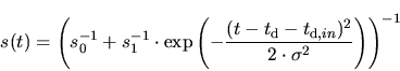
This time-step behavior is implemented using the following equation:
 |
(6.5) |
 |
(6.6) |
| (6.7) |
![\resizebox{0.95\textwidth }{!}{
\psfrag{xlabel} [ct][ct] {time $t$\ (ps)}
\psfra...
...udegraphics[width=0.95\textwidth ]{../figures/timesteprefinement-gatedelay.eps}}](img204.gif)
|