
 |
|
||||
BiographyLuiz Felipe Aguinsky was born in 1990 in Porto Alegre, Brazil. He received his Bachelor's degree in Physics from the Federal University of Rio Grande do Sul (BSc, 2013). Subsequently, he studied Simulation Sciences at RWTH Aachen University (MSc, 2018), having written the Master's thesis at the German Aerospace Center. After finishing his studies he joined the Institute for Microelectronics in March 2018, where he is currently working on his doctoral degree. He is researching high performance numerical approaches for Technology CAD within the scope of the Christian Doppler Laboratory for High Performance TCAD. |
|||||
Simulating the Fabrication of Silicon Microcavity Optical Resonators
Optical resonators are important tools for fundamental science, having many applications in diverse fields, such as metrology, laser physics and quantum information processing. Recently, an approach to fabricating optical resonators has been developed using a complementary metal oxide semiconductor compatible process flow. This is achieved using a two-step isotropic plasma etching process. The first etching step is performed in the presence of a photoresist with circular openings. After its stripping, a second etching step widens the cavities to achieve the desired profiles. In order to reduce roughness, an oxidation step is performed on the resulting wafer.
Process modeling provides invaluable insight into this fabrication process. Using the simulation tool, ViennaTS, we have successfully modeled the two-step etching process. The state of the simulation after the first etching step is represented in Fig. 1. After thorough investigation, we have determined the adequate minimal model for reactive transport. The profile is adequately replicated using a single effective particle with multiple isotropic reflections, in addition to an isotropic source distribution. This simulation workflow allows for the description of the surface at every step of the fabrication process, thereby complementing the experiment, which only records the final surface.
The first challenge after model discrimination is the calibration of the model. In Fig. 2, we show the manual calibration of the simulation parameters required to recapture the final profiles measured by atomic force microscopy (AFM). Our free parameters are the etch rates for both steps and the sticking coefficient, which is the particle reflection probability. We note that to achieve the best fit, the second etch rate must be lower than the first. This is to be expected since during the second step, more of the wafer's surface is exposed to consume reactants, in an effect known as reactor loading.
Our research currently includes using these calibrated simulations to provide insight into process optimization. The current challenge is obtaining the optical quality parameters from the simulation data as we vary the process parameters. To achieve this, we need to move away from a manual calibration approach towards a method for automatic parameter extraction. We are investigating the use of tools and algorithms from the field of computer vision to aid us in this task. In Fig. 3, we illustrate how we have used the circular Hough transform, as implemented in the OpenCV library, to extract the radius and position of the cavity opening. Remarkably, this can be achieved even with incomplete data. We aim to develop a robust framework to automatically calibrate our simulations and to extract the optimized optical parameters, showcasing the power of process simulations.
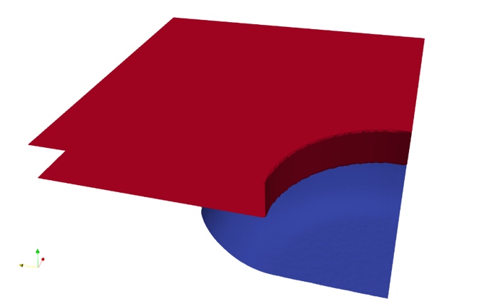
Fig. 1: Simulated profile at the end of the first etch process showing the silicon microcavity (blue) and photoresist (red). Only one quarter of the domain needs to be simulated due to the use of reflective boundary conditions. The simulation tool is ViennaTS.
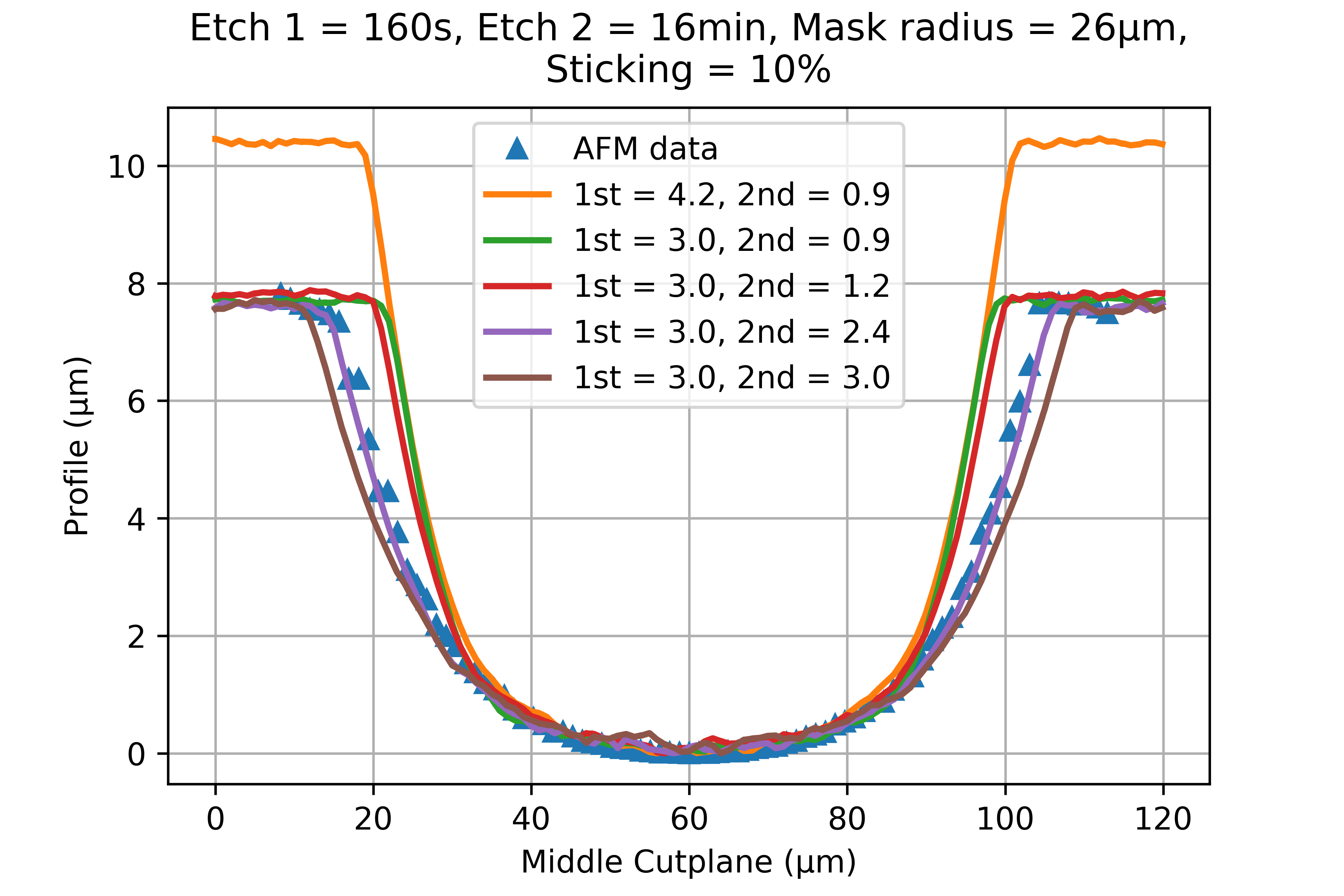
Fig. 2: Manual calibration of the simulation to the AFM data points (blue). Here, we show that good agreement can be obtained (purple) by considering the effects of reactor loading, i.e. the reduction of the etch rate on the second step.
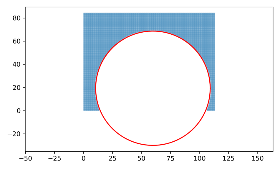
Fig. 3: Automatic detection of the cavity opening radius (red) from the data (blue). Using OpenCV, we can extract features from the data even with incomplete information.