
 |
|
||||
BiographyHajdin Ceric was born in Sarajevo, Bosnia and Herzegovina, in 1970. He studied electrical engineering at the Electrotechnical Faculty of the University of Sarajevo and the Technische Universität Wien, where he received the degree of Diplomingenieur in 2000. In 2005 he received his PhD in technical sciences and in 2015 his venia docendi in microelectronics from the Technische Universität Wien. In 2010 he was appointed the head of the Christian Doppler Laboratory for Reliability Issues in Microelectronics. He is currently an Associate Professor at the Institute for Microelectronics. His research interests include modeling and simulation of reliability issues in interconnects for ultra large-scale integration. |
|||||
Statistical Simulations of Nano-Interconnect Reliability
The reliability of interconnects is affected by a complex degradation process driven by several forces each of which has been ever-present since the historical beginning of interconnect technology. These forces include electromigration, stressmigration and thermomigration. These driving forces induce a transport of material within the interconnect metal that damages the crystal structure and causes the formation of intrinsic voids. The increase in the metal's resistance due to this migration and growth of intrinsic voids leads to interconnect failure. It is important to note that thermomigration in metal interconnects is not the only problem associated with the thermal budget of integrated circuits (ICs). The heat produced by Joule heating in the interconnects - in addition to the heat produced by other devices - induces thermomechanical stress throughout the ICs and also affects the reliability of the transistors within the IC.
A typical nano-interconnect layout is presented in Fig. 1. Cu metal is wrapped in a Ti- or Ta-based alloy in order to prevent copper migration into the neighboring dielectric. The top surface of the interconnect metal is covered by the etch-stop/capping layer. Originally silicon-nitride was used for capping, but numerous other materials have since been tested in this role. To slow down material transport along the top surface of the interconnect, an additional layer may be added (Co). The whole structure is packed into a dielectric; originally silicon-oxide, but nowadays a plethora of different low-k materials are utilized.
As the linewidth of interconnects decreases, the importance of material transport along grain boundaries (GBs) and interfaces increases. Thus, the lifetime of interconnects becomes more sensitive to the values of the parameters that determine this transport, such as effective valences and diffusivities. The interconnect linewidth has an impact on interconnect resistivity and the effective valence, which also needs to be considered. The material transport is additionally determined by the GB distribution and the orientation of single grains. The metallic microstructure in a given interconnect is influenced by the specific process conditions, choice of materials and interconnect dimensions.
In the case of typical microstructures for nano-interconnects, two additional aspects need to be considered. First, the microstructure strongly depends on the interconnect thickness. Second, due to the increased temperatures during operation, the microstructure may undergo transformations. Experimental SEM/FIB/EBSD studies of interconnect microstructure provide the grain size distribution and the crystal orientations inside grains. These studies show that the grain sizes inside Cu interconnects are distributed according to a log-normal distribution and tend to be dominated by several different crystal orientations. Some earlier investigations have led to the conclusion that the statistical properties of interconnect failure times follow the statistical properties of the interconnect microstructure.
In our approach, we subject the microstructures extracted from the SEM images of real interconnects used for accelerated electromigration tests to numerical simulations. The method itself is schematically presented in Fig. 2, where a 2D network of GBs is extruded into prismoidal shapes and cut into the 3D interconnect geometry. A simulation is then performed, and in accordance with the experimental observations, a log-normal distribution of failure times is obtained (Fig. 3).
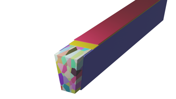
Fig. 1: Typical modern interconnect structure: Polycrystal Cu is wrapped around all sides, except the top, with liner metal (blue). The top surface is covered by Co (yellow) and by the etch-stop layer (red).
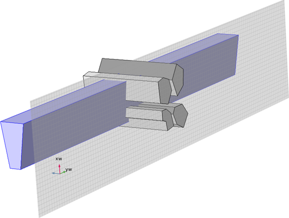
Fig. 2: An example of projecting and cutting the planar microstructure into the 3D interconnect geometry, which is then used for simulations.
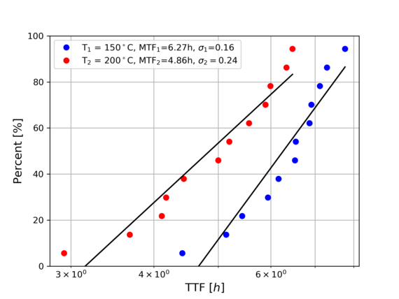
Fig. 3: Results of statistical simulation of electromigration failure times for two temperatures and 12 different microstructures.