
 |
|
||||
BiographyAl-Moatasem El-Sayed was born in Sheffield, United Kingdom in 1988. He completed his Masters in chemistry at the University of Manchester in 2010. He went on to do his Ph.D in physics at University College, London, focussing on atomistic modeling of point defects in oxides. He then joined the Institute of Microelectronics in June 2015, his current research interests are modeling of point defects in oxides and their effect on electronic devices. |
|||||
Atomistic Modeling of Point Defects in Silicon-Germanium Based Devices
Computer simulations are an invaluable tool to help us understand and improve electronic devices. Due to the extraordinarily small dimensions of modern electronic devices, their properties can be affected by small changes in the system at an atomic level. We therefore focus on using atomistic simulations of materials to calculate the relevant properties for electronic device issues. In particular, my research uses state-of-the-art density functional theory codes to identify relevant point defects and their mechanisms in semiconductors and oxides.
Point defects have been identified as a source of reliability issues in electronic devices across a range of materials. New material combinations are now employed to improve electronic properties and achieve faster switching than in silicon-based devices. As is expected, defects also play an important role in devices based on novel material combinations. However, it is usually unknown whether these defects are analogous to those seen in silicon-based devices or whether they are completely different.
Our recent work explores the atomistic origins of reliability issues in devices based on silicon-germanium alloys. Starting from atomistic models of amorphous silicon dioxide, we create models of amorphous germanium dioxide. The total structure factor, an experimentally measurable quantity, agrees rather well with the simulated structures, as can be seen in Fig. 1. The chemical composition of these structures was then altered to reflect varying concentrations of silicon-germanium alloys. Point defects analogous to those in silicon-based devices were then introduced. These included oxygen vacancies, electron traps and silicon or germanium bonds with hydrogen. We found that many of these defects had analogs in silicon-germanium oxides. An example of an oxygen vacancy in an alloy with a high germanium concentration is shown in Fig. 2. Curiously, it was found that the behavior of the defects varied with the germanium content, with some defects disappearing entirely from the structures. These results can help explain the differences in reliability issues in silicon and silicon-germanium based devices.
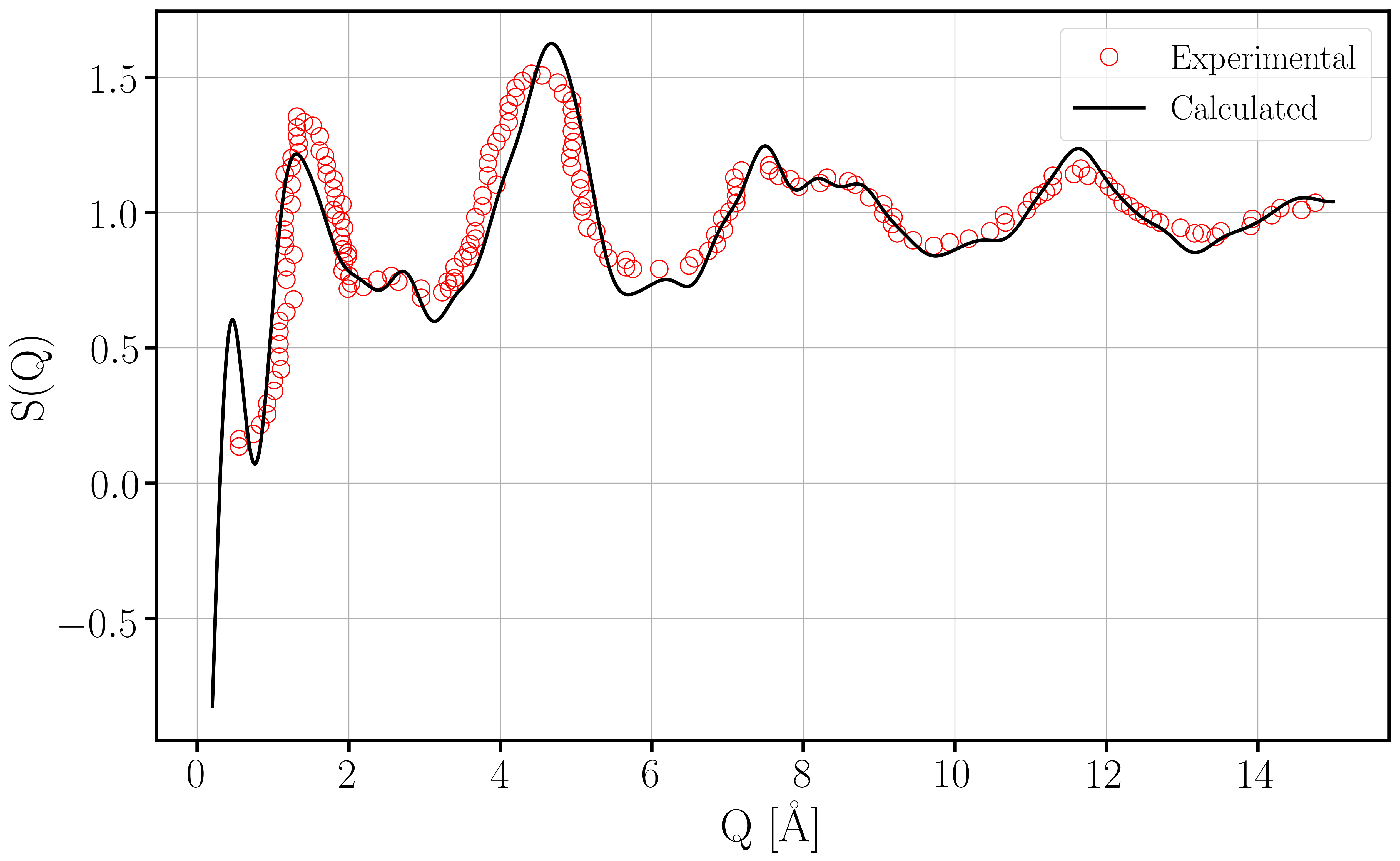
Fig. 1: The total structure factor of our simulated amorphous germanium dioxide structures compared to experimental results.
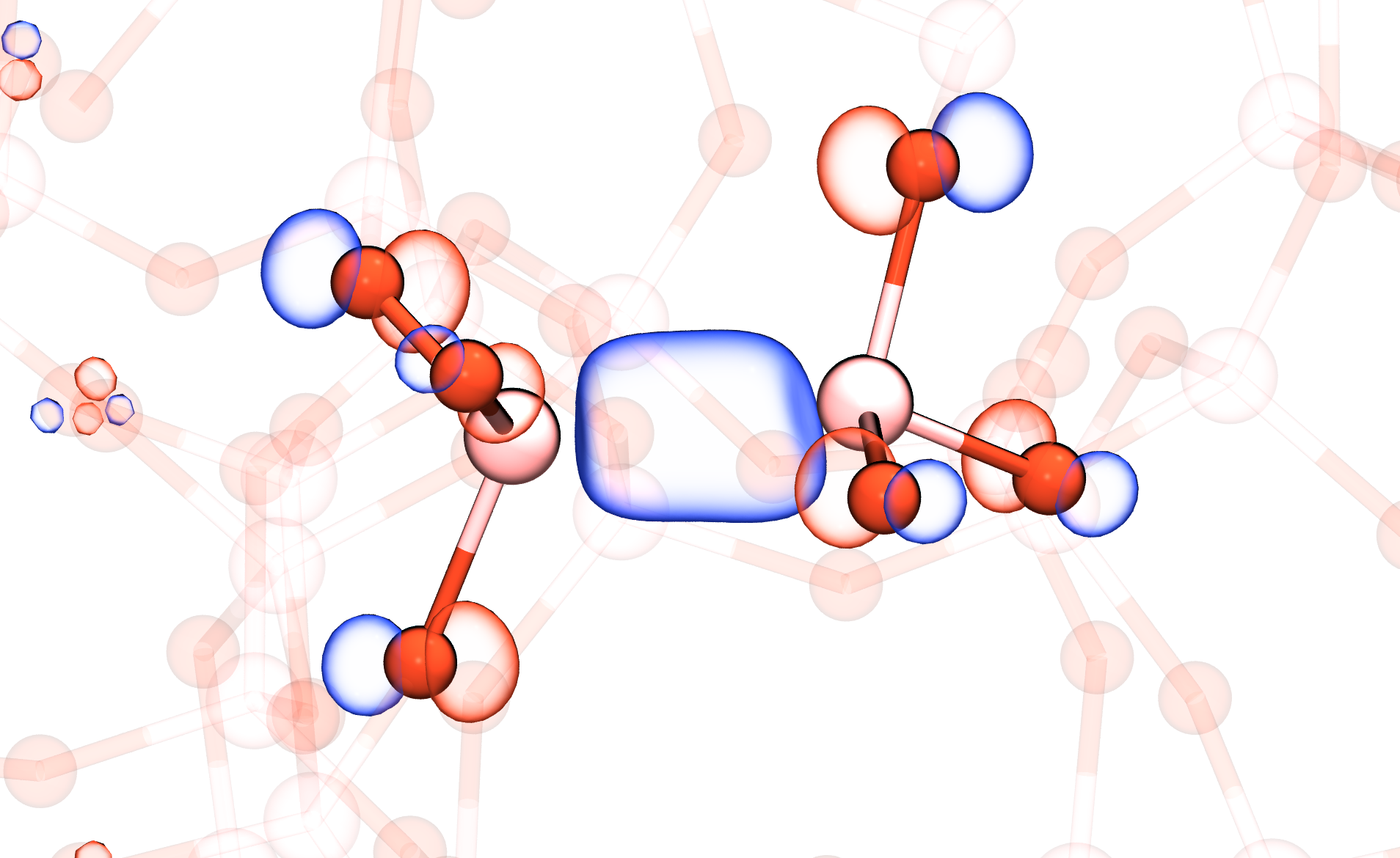
Fig. 2: The oxygen vacancy in a silicon-germanium dioxide that has a high germanium concentration. The germanium atoms are shown in pink and the oxygen atoms in red. The blue isosurface represents the highest occupied orbital of the system, which sits in the band gap and is highly localized around the vacancy.