
 |
|
||||
BiographyYury Illarionov was born in Leningrad (now Saint-Petersburg) in 1988. He studied solid state physics at the Physical Science and Technology Faculty of St. Petersburg State Polytechnical University where he received the B.Sc. and M.Sc. degrees in 2009 and 2011, respectively. From 2010 to 2012 he studied advanced material science in Grenoble Institute of Technology (France) and University of Augsburg (Germany) in frameworks of Functionalized Advanced Materials and Engineering (FAME) Erasmus Mundus program and in September 2012 received a double European M.Sc. degree. His scientific carrier has started in October 2007 in Ioffe Physical-Technical Institute (Russia) and in November 2011 he joined the PhD program there. He also visited IRCELYON (France, May-July 2011) and Singapore Institute of Manufacturing Technology (Singapore, February-July 2012) as a young guest researcher. He joined the Institute for Microelectronics in February 2013. In January 2015 he received the PhD degree in semiconductor physics from Ioffe Physical-Technical Institute and in December 2015 the Dr.techn. degree from TU Wien. Since January 2016 Dr. Yury Illarionov is a postdoc researcher working on reliability of the next-generation 2D FETs with graphene, MoS2 and phosphorene. |
|||||
Stability of Flexible MoS2 FETs with Parylene N/Al2O3/Parylene N Encapsulation
Encapsulation of molybdenum disulfide (MoS2) field-effect transistors (FETs) presents an important step towards top-gated devices that are required for circuit integration. This is because the insulators employed to protect the channel from the ambient environment can be subsequently scaled and used as top-gate insulators. However, encapsulation layers themselves can also degrade device performance. For example, encapsulation can increase device-to-device variability, reduce the mobility or cause undesired shifts in the threshold voltage. We have recently attempted to understand the impact of the encapsulation scheme on the performance and stability of MoS2 FETs with a 30 nm thick Al2O3 gate insulator (Fig. 1a) grown by atomic layer deposition.
To do this, we studied the devices encapsulated using four different schemes, namely Al2O3, Al2O3/Parylene N, Parylene N/Al2O3/Parylene N and Parylene C/Al2O3/Parylene N (Fig. 1b). In all cases, the growth of Al2O3 was performed at 200 oC, while Parylene N or C was deposited after 3 hours of annealing at 130 oC followed by 12 hours of pumping. Similar to previous literature, our results show that the ID-VG characteristics of MoS2 FETs with Al2O3 encapsulation have a strongly negative Vth (Fig. 2a) due to the n-type doping of the channel by positive charges inside the Al2O3. At these negative gate voltages, there is a substantial thermionic leakage current, which leads to a reduced on/off current ratio of only about 106. In contrast, the use of Parylene N/Al2O3/Parylene N encapsulation makes Vth considerably more positive and thus allows one to achieve on/off ratio values of up to 1010 (Fig. 2b). Furthermore, our MoS2 FETs with Parylene N/Al2O3/Parylene N encapsulation are not sensitive to the ambient environment and exhibit excellent stability after annealing at 165 oC (Fig. 2c), as well as the smallest variability in performance parameters. Thus, the use of a Parylene N/Al2O3/Parylene N encapsulation scheme offers an important step towards highly stable MoS2 FETs. However, further steps are required to optimize device processing by avoiding air exposure in between device fabrication and encapsulation.
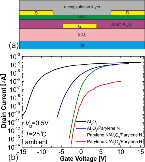
Fig. 1: (a) Schematic layout of our MoS2 FETs. (b) Typical ID-VG characteristics of our devices with different encapsulation schemes. Pure Al2O3 introduces a strong negative shift of Vth.
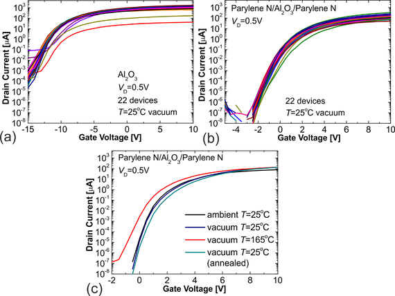
Fig. 2: ID-VG characteristics of 22 devices with (a) Al2O3 and (b) Parylene N/Al2O3/Parylene N. The use of Parylene N makes Vth more positive, which results in on/off current ratios of up to 1010. (c) Simultaneously, the ID-VG characteristics of Parylene N/Al2O3/Parylene N encapsulated devices remain similar in the ambient environment and in the vacuum before and after annealing.