
 |
|
||||
BiographyTheresia Knobloch was born in Vienna in 1992. She received her BSc degree in Technical Physics and the degree of Diplomingenieur in Microelectronics from the Technische Universität Wien in 2014 and 2016, respectively. She joined the Institute for Microelectronics in April 2016, where she is currently working on her doctoral degree. Her current research topic are novel devices based on two-dimensional materials. |
|||||
Modeling the Transfer Characteristics of MoS2 FETs with an Ultrascaled CaF2 Gate Insulator
Two-dimensional (2D) materials, such as molybdenum disulfide (MoS2), hold the promise of complementing or even outperforming silicon-based field-effect transistors (FETs) in future generations of ultrascaled computer chips. MoS2 is a semiconductor and can thus be used to form the channel of the transistor. The main advantages of MoS2 and other layered semiconductors are their dangling bond free interface due to the van der Waals bonds between adjacent layers and their sizable mobility even within the scaling limit of one monolayer. In order to fully exploit the potential of 2D semiconductors, however, they have to be paired with suitable gate insulators. A suitable insulator has to satisfy two requirements. First, it should form a high-quality, ideally defect-free interface with the 2D layer, and second, it has to demonstrate good scaling properties. This means that the insulator needs to have a high dielectric constant, a large band gap and can be fabricated in the form of a very thin layer. The crystalline material calcium fluoride (CaF2) satisfies these requirements, as thin layers can be grown using chemical vapor deposition and molecular beam epitaxy and because of its reasonably high dielectric constant of 8.43 and its wide band gap of 12.1eV. In addition, its inert surface is terminated with fluorine atoms, which allows for van der Waals bonding with the MoS2 layer on top.
Here, we studied the device operation of prototype MoS2 FETs on CaF2 based on bilayer MoS2 transferred to a 2 nm CaF2 insulator grown on a (111) silicon wafer that serves as a global back gate. Source and drain electrodes are formed using Ti/Au contacts deposited on top of the device. We measured the transfer characteristics of the devices and modeled the current flow through the devices using a drift-diffusion based technology computer-aided design (TCAD) model. In Fig. 1, the transfer characteristics are denoted by the circles, representing measurement points, and the lines, showing the simulated curves.
For these prototype devices, where the channel and the contact regions are both undoped and the Fermi level of the metal source and drain contacts is pinned within the gap, the Schottky barriers formed between the metal and the semiconductor dominate the current flow. The current over the Schottky barriers has two contributions, the thermionic emission of charges over the barrier and the field emission or tunneling through the barrier. The impact of the Schottky barrier on carrier transport depends strongly on the barrier thickness, which is approximated by the screening length, Λ. In Fig. 2, the simulated curves are compared when including the Schottky barriers at the contacts and for purely Ohmic contacts. Because of the very thin semiconductor and insulator layers in this case, the Schottky barrier is very thin, allowing for high tunnel current contributions, meaning that the Schottky barriers do not degrade the sub-threshold slope of the device.
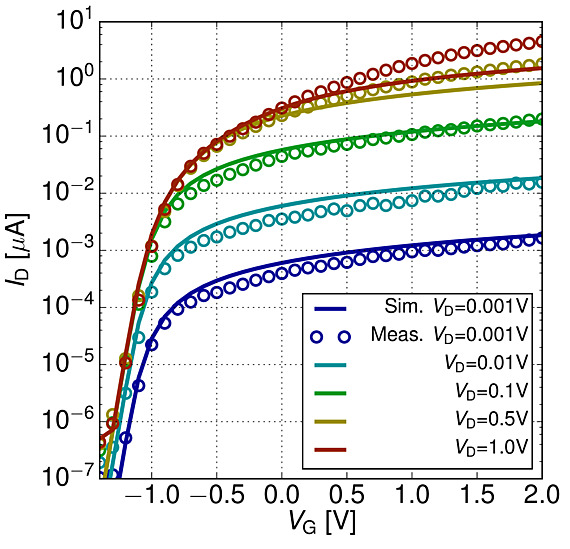
Fig. 1: Transfer characteristics of our MoS2/CaF2 FETs. The symbols denote measurement points, and the lines were simulated using a drift-diffusion based TCAD framework.
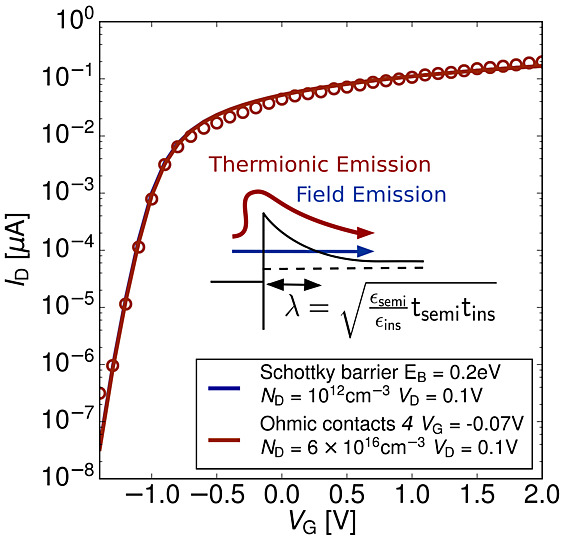
Fig. 2: A comparison of the simulated characteristics with and without including the injection of charge carriers over Schottky barriers at the source and drain contacts. Without Schottky barriers, the difference in the charge carrier density has to be corrected for by increased doping. Due to the thin semiconductor and insulator layer and the subsequently thin barrier, the barrier does not decrease the sub-threshold slope.