
 |
|
||||
BiographyAlexander Makarov was born in Volgograd, Russia, in 1985. He studied information technology at the Volgograd State Technical University, where he received the BSc degree in 2006 and MSc degree in 2008. He joined the Institute for Microelectronics in October 2009 and has obtained the doctoral degree in March 2014. He is currently employed as a post-doc researcher. His scientific interests include Monte-Carlo simulations and nonvolatile memory device modeling. |
|||||
Bi-Modal Variability of nFinFET Characteristics During Hot-Carrier Stress: A Modeling Approach
In scaled field-effect transistors (FETs) with dimensions that have been shrunk beyond the sub-decananometer range, sample-to-sample variability in device characteristics becomes an important issue. Such statistical spread can be due to various reasons, including fluctuations in the oxide thickness, disorder at the semiconductor/dielectric interface, work-function variations and the random placement of doping atoms. Although in mature technologies, the first three concerns are mitigated, the problem of random dopant (RD) variability still persists and has been reported by semiconductor manufacturers. Moreover, a deterministic description of reliability issues in short-channel devices is not sufficient because degradation is driven by the generation of discrete random traps (RTs), which results in time-dependent variability of device characteristics.
Among reliability issues, hot-carrier degradation (HCD) has repeatedly been reported to be the most detrimental. Nevertheless, there are a very limited number of papers presenting experimental investigations of variability induced by HCD. The few modeling approaches to HCD variability that exist are limited to phenomenological descriptions and do not address the overarching complex physical picture.
To bridge this gap, we have performed a statistical analysis of the cumulative impact of randomly generated (during hot-carrier stress) traps and random dopants on nFinFET characteristics. Calculations were performed at high stress voltages and for conditions close to the operating regime. We generated 200 different configurations of devices with RDs and subsequently solved the Boltzmann transport equation to obtain the continuous interface trap concentration. These deterministic densities for each individual configuration were then randomized and converted to 200 different configurations of RTs, yielding a total of 40,000 samples for our study. Analysis of these showed that at high stress voltages (with both RTs and RDs taken into account) probability densities of linear drain currents and device lifetimes are close to a bi-modal normal distribution, while in the operating regime, such a trend is not visible (Fig. 1). This hinders projections to operating conditions and lifetime extrapolations and suggests that stochastic treatment of HCD is needed.
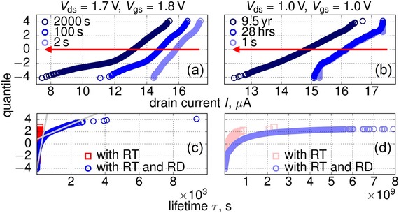
Fig. 1: (a, b) Probit plots of Id,lin distributions computed with the impact of RTs and RDs taken into account. (c, d) Probit plots of device lifetime distributions obtained with only the impact of RTs (square symbols) considered versus the cumulative effect of both RTs and RDs (circles).