
 |
|
||||
BiographyChristian Schleich started his engineering career as a service engineer and technical support engineer at EVGroup, a semiconductor equipment supplier, directly after graduating from technical high school (HTL) in 2006. He studied electrical engineering at TU Wien, where he received his BSc degree in 2017 and his MSc degree in 2019. He joined the Institute for Microelectronics in February 2019 and is currently working on his PhD on the characterization and modeling of defects in SiC MOS transistors. |
|||||
Modeling of SiC Transistors
Transistors fabricated on 4H-SiC substrates show superior properties, such as reduced resistance for a given blocking voltage, making them very attractive for application as switches in power conversion electronics. The performance of SiC metal–oxide–semiconductor field-effect transistors (MOSFETs) in general can still not yet be completely exploited due to a higher density of defects, however, which occur in the vicinity of the interface between bulk SiC and SiO2. These defects give rise to a distinct hysteresis in the transfer characteristics and lead to an increased drift in the threshold voltage (i.e. bias temperature instabilities) compared to what is observed for established Si devices. This makes an accurate time-to-failure analysis of SiC power devices very challenging.
To characterize the impact of these defects on device performance, we have carefully analyzed lateral channel SiC MOSFETs utilizing measure-stress-measure (MSM) schemes. To explain experimental data, we performed physics-based device simulations employing our one-dimensional reliability simulation framework, Comphy. This tools allows us to efficiently compute the impact of a large set of single defects on device characteristics (e.g. the threshold voltage) by employing a two-state nonradiative multi-phonon defect model. Using this approach, we are able to extract defect bands for electron and hole trapping, which allows for a proper explanation of measured device degradation with a physical model, which had not been done previously.
Our simulations suggest that charge trapping in SiC transistors is dominated by electron traps with thermodynamic trap levels in the vicinity of the conduction band edge of SiC that are responsible for both fast and also slow recovery behavior corresponding to the device's degradation. The fast electron traps are further responsible for the hysteresis observed during voltage sweeps, while the slow electron traps are the origin of the long-term degradation of Vth. We have also compared the trap levels of a variety of defect candidates, which have been extracted by ab-initio methods in combination with electron spin resonance experiments. Although many suitable defect candidates are proposed in a number of publications, no specific defect candidate could be ruled out as the main culprit for charge trapping in these devices. Furthermore, based on the simulator calibration, the first physics-based lifetime prediction in SiC MOSFETs has been presented.
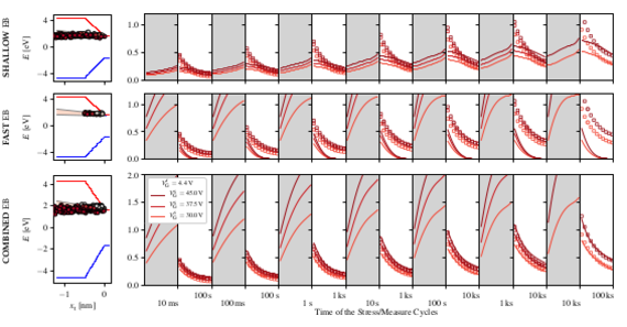
Fig. 1: Measured (circles) ∆Vth utilizing eMSM sequences at different VG,s and at constant VG,r = 4.4 V at T = 30 C and (top) simulation results (lines) considering a
shallow electron trap band (EB) originating from border traps as extracted previously for Si/SiO2 technology. The simulation explains the tails of the recovery data measured after
large stress times well, whereas the fast recovery behavior is not sufficiently explained by the shallow EB. (middle) A fast EB accounts for a large fraction of
the recovery data measured within the first few decades immediately after stress release. This contribution can be ascribed to near interface traps arranged in the transition
region between the substrate and oxide. (bottom) The combination of both defect bands shows good agreement with experimental data, especially for long stress and recovery times.
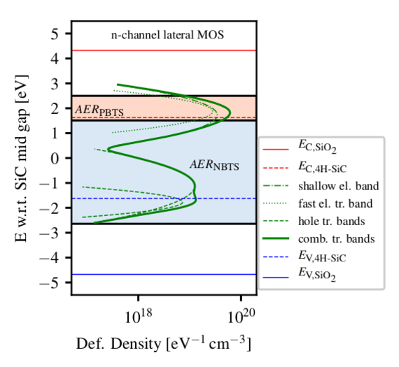
Fig. 2: Defect densities within the first 5 Å from interface. Extracted densities cover the main features of those
extracted by experiments, like the steep increase towards EC,SiC.
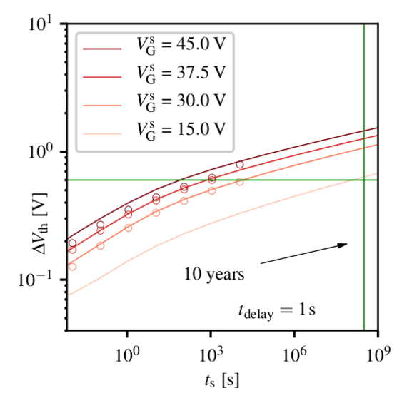
Fig. 3: Accurate lifetime extrapolation from our calibrated simulation environment reveals an overall ∆Vth ≈ 0.6 V at
operating conditions VG,s = 15 V for a lifetime of 10 years.