
 |
|
||||
BiographyBernhard Stampfer, born in 1989 in Austria, studied at the Technische Universität Wien where he received the BSc degree in Electrical Engineering (2013) and the Diplomingenieur degree in Microelectronics and Photonics (2016). He joined the Institute for Microelectronics in March 2016, where he is working on his doctoral degree. |
|||||
Statistical Characterization of Oxide Defects in a Scaled Technology
In modern metal–oxide–semiconductor field-effect transistors (MOSFETs), scaling has led to increased variability among seemingly identical devices. The main culprits for this significant device-to-device variation are atomistic defects in the oxide that are also the root cause of a number of further detrimental effects. In devices with large gate areas, thousands of these defects exist, and thus, the drift of the device's threshold voltage is found to be relatively similar among formally identical devices. In nanoscale devices, however, the oxide contains only a handful of defects, and their individual impact on the device's behavior is strongly magnified. The statistical variation in the number of defects between individual small devices gives rise to considerable device-to-device variation, where some devices can degrade much faster than others. This behavior is especially detrimental for high-performant operation of integrated circuits, where millions of such transistors have to behave within a defined envelope of parameters to ensure the proper functioning of the chip.
Considering these variations, it is evident that studying the reliability of such scaled devices requires the characterization of many devices to obtain a clear picture of the average device behavior and its deviations. A custom designed chip, where single devices are arranged in an array-like manner, has been developed specifically for this task. Using this chip, we perform experiments on thousands of individual devices to study the impact of various operating conditions on a commercial high-k technology. By using a statistical approach based on a defect-centric model, we can evaluate the large amount of data obtained from the measurements on the array chip very efficiently. Furthermore, technology computer-aided design simulations using the nonradiative multi-phonon model have been performed and allow us to replicate the measured results and extrapolate them to a 10-year timeframe.
In Fig. 1, results for devices with a gate width of 100 nm and length of 30 nm are shown. The devices are high-k metal gate pMOSFETs, manufactured in a commercial technology. Shown are the average step heights of the defects (crosses), the average number of defects causing random telegraph noise (RTN) (diamonds) and the average number of charged defects (circles). While the average step heights and RTN-active defects are not affected by stress, the number of charged defects strongly depends on the stress biases and stress time.
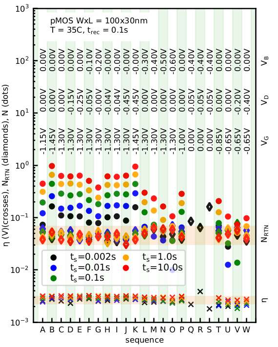
Fig. 1: Results for the average step heights of the defects, the average number of RTN-active defects, NRTN, and the average number of defects, N, which capture a charge after phases of stress at various stress times, ts.