
 |
|
||||
BiographyViktor Sverdlov received his Master of Science and PhD degrees in physics from the State University of St.Petersburg, Russia, in 1985 and 1989, respectively. From 1989 to 1999 he worked as a staff research scientist at the V.A.Fock Institute of Physics, St.Petersburg State University. During this time, he visited ICTP (Italy, 1993), the University of Geneva (Switzerland, 1993-1994), the University of Oulu (Finland,1995), the Helsinki University of Technology (Finland, 1996, 1998), the Free University of Berlin (Germany, 1997), and NORDITA (Denmark, 1998). In 1999, he became a staff research scientist at the State University of New York at Stony Brook. He joined the Institute for Microelectronics, Technische Universität Wien, in 2004. His scientific interests include device simulations, computational physics, solid-state physics, and nanoelectronics. |
|||||
The Electronic Structure of Topological Insulator Nanoribbons
Topological insulators belong to a new class of semiconducting materials with an unusual band structure. As in a normal dielectric, the conduction and the valence bands are separated by a band gap, but the order of those bands is inverted such that the valence band edge lies above that of the conduction band. As the conventional band order must be restored when a topological insulator is interfaced with a normal dielectric, a band crossing must appear close to the interface, which results in the emergence of edge states with energies lying in the gap between the bands of the topological insulator. The edge states then possess a linear Dirac-like energy dispersion. In addition, the edge states are topologically protected by time-reversal symmetry, which results in electron propagation without backscattering. This property makes them attractive as a material for highly conductive transistor channels.
A 1T’ phase of MoS2, a promising material for future microelectronic devices, is shown to be a two-dimensional (2D) topological insulator, with the band structure shown in Fig. 1. By applying a vertical electric field Ez, the inverted gap at one of the points ky= k0 and ky=-k0 can be reduced, closed and opened again as a direct dielectric gap in the sheet. If the gap becomes direct, no propagating edge states are allowed, and the current can be terminated.
In order to enhance the on-current through the channel, it is beneficial to have many edges by stacking several narrow nanoribbons. The subband structure in a narrow nanoribbon of 1T’ molybdenum disulfide evaluated with an effective k∙p Hamiltonian is shown in Fig. 2. Highly conductive topologically protected edge states with a nearly linear dispersion are clearly seen. Due to the interaction of the edge modes located at opposite edges, a small gap in their linear spectrum opens in a narrow nanoribbon (Fig. 2). This gap increases with the strength of the perpendicular out-of-plane electric field produced by the gate voltage, in contrast to the behavior in a wide ribbon. The increase of the gap between the subbands with the gate voltage is expected to result in an abrupt decrease in current. The current dependence on the gate voltage can be used for designing nanoribbon-based current switches.
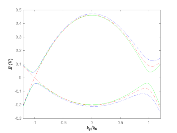
Fig. 1: Bulk energy dispersion in 1T’-MoS2, a 2D material. The solid green curves display the gaps at ky= k0 (solid green curves). Increasing the electric field closes the gap (dashed red curves) and reopens it again as a direct gap (dotted-dashed blue curves).
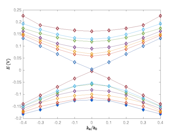
Fig. 2: Subband structure in a narrow nanoribbon of 1T’-MoS2. The subbands with an almost linear dispersion corresponding to the topologically protected edge states are observed.