
 |
|
||||
BiographyAlexander Toifl was born in St. Pölten, Austria, in 1993. He studied at the TU Wien where he received the BSc. degree in Electrical Engineering (2016) and the Diplomingenieur degree in Microelectronics and Photonics (2018). He joined the Institute for Microelectronics in August 2018 as a research assistant. Alex's scientific interests include computational modeling (post-implantation annealing of GaN and SiC) and high performance numerical approaches (non-planar epitaxy) for process TCAD. |
|||||
Simulating Anisotropic Wet Etching and Non-Planar Epitaxial Growth
Anisotropic wet etching and non-planar epitaxy are semiconductor fabrication techniques that are characterized by highly crystal-orientation-dependent etch/growth rates. In their description by the level-set method, the anisotropy leads to a non-convex Hamilton-Jacobi equation. As a consequence, unstable surface propagation may emerge, leading to unphysical results. We have developed a calibration-free Stencil Lax-Friedrichs scheme and an advanced adaptive time-stepping approach, tailored to the level-set speed functions associated with anisotropic etching and epitaxy. The scheme calculates the numerical dissipation based on information about the local geometry and the nature of the etch rates/growth function, which enables an optimized trade-off between overly rounding sharp geometric features and stable surface propagation.
We integrated the Stencil Lax-Friedrichs scheme into the topography simulator, ViennaTS. Fig. 1(a) shows the simulation result of an Si cavity etch, as is typically employed for cantilever structures. In particular, the etch rates along the <111> direction are significantly smaller than the rates along <100>, resulting in a topography defined by {111} planes. The developed stabilization scheme can be employed within a multi-step topography simulation, as demonstrated in Fig. 1(b).
Furthermore, we introduced the deposition top layer method, which allows for robust handling of multiple material regions in non-planar epitaxy simulations. In order to demonstrate the deposition top layer, we considered a three-dimensional fin structure, which forms the geometrical basis of modern fin field-effect transistors (FinFETs). A crucial process step during the fabrication of a FinFET is heteroepitaxial growth of silicon-germanium (SiGe) on top of the Si fin. Similar to crystallographic wet etching, the growth rates of epitaxial SiGe are strongly anisotropic, with a minimum along the <111> direction. Consequently, {111} crystal facets dominate the growth of the crystal, and a SiGe diamond on top of the Si fin is formed. Fig. 2 shows the fully formed SiGe diamond, which is characterized by the geometric parameters of the overgrowth height and the lateral length. We have compared these parameters to the ideal values, showing that the Stencil Lax-Friedrichs scheme enables stable surface propagation with the correct growth rates.
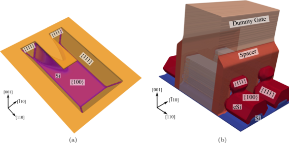
Fig. 1: (a) Cavity etch producing a free cantilever for sensor applications. The Si substrate is anisotropically etched with a wet etchant, e.g. KOH. (b) Advanced-node stacked nanosheet geometry with epitaxially grown source and drain (red). Silicon crystal facets are labeled, showing the resulting complex geometries due to the epitaxial growth.
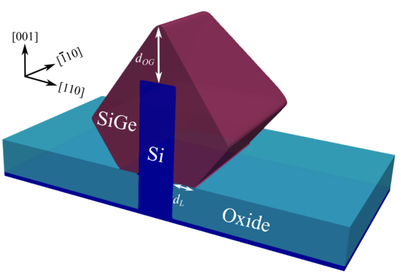
Fig. 2: SiGe is heteroepitaxially grown on Si forming {111} facets. The Stencil Lax-Friedrichs scheme and the deposited top layer enable stable and robust epitaxial growth in three-dimensional level-set simulations.