
 |
|
||||
BiographyMichael Waltl was born in Oberndorf near Salzburg, Austria. He received the BSc degree in electrical engineering, the degree of Diplomingenieur in microelectronics, and the doctoral degree in technical sciences from TU Wien in 2009, 2011, and 2016, respectively. His scientific focus is on experimental characterization and modeling of reliability issues prevalent in semiconductor devices and devices with more exotic 2D materials. In this field, he primarily studies bias temperature instabilities in modern transistors. He also leads the device characterization laboratory at the institute, where he is in charge of developing electrical measurement methods. |
|||||
Ultra-Low Noise Measurements for the Evaluation of the Distribution of Defects in Transistors
The performance and also the geometry of integrated metal-oxide-semiconductor (MOS) transistors have been continuously improved over recent years. This successful development has led to the fact that electronic devices based on complementary MOS (CMOS) technology have become indispensable in our everyday life. Despite these improvements, however, all MOS transistors suffer from imperfections at the atomic level that can emerge as electrically active sites, so-called defects. These defects are unavoidably introduced during device fabrication and occur at interfaces between materials with different lattice constants (i.e. at the interface between the substrate and the insulator). Furthermore, these defects can become charged and uncharged during device operation, leading to a drift in the threshold voltage of MOS transistors and a reduction of their sub-threshold slope. The defects are also responsible for the alteration of the carrier mobility and cause an increase in the on-resistance of the respective devices.
To study the impact of such defects on semiconductor transistors, bias temperature instabilities and hot-carrier degradation are among the most extensively studied phenomena and also the most significant in determining the time-to-failure of devices. Both effects have in common that they occur at nominal operating conditions and diminish the performance of every single transistor. To study these phenomena, typically changes in the IDVG characteristics or drifts in the threshold voltage are monitored and analyzed. Quite interestingly, charge transitions are observed as discrete steps in measurement data when highly scaled devices are investigated, while continuous trends are observed in large-area transistors. By studying the charge trapping kinetics of single defects employing scaled devices, the physical mechanisms behind charge trapping can be investigated in detail. In addition to the understanding of single defects, however, the analysis of the statistics of many defects present in a transistor is also important for the evaluation of a certain technology. For this, the complementary cumulative distribution function (CCDF) of step heights can be created and analyzed.
To create the CCDF of step heights, single charge emission events from a number of recovery traces, recorded after each of the devices has been stressed at relatively high gate bias, are extracted, as shown in Fig. 1. In order to account for device-to-device variations in the recording of recovery traces from a large set of devices, the recovery gate bias is selected using a constant current criterion applied to IDVG characteristics measured prior to the stress phase. As can be seen from the results, the charge emission times are distributed over many decades in time and also show widely distributed step heights. By comparing the measurement resolution of our instrument with recently published data, it was found that achieving a measurement resolution below a few nanoampere for single charge transitions is typically difficult to achieve with general-purpose instruments. A high measurement resolution is essential for single defect characterization, however, otherwise many defects will be missed in the analysis (see Fig. 2). In order to achieve a high measurement resolution, we employ our custom-made defect probing instrument in combination with lead batteries, which provide the power supply for the analog circuitry.
The ability to perform ultra-low noise measurements is even more essential when the CCDFs of step heights of nMOS transistors are analyzed (see Fig. 3). In general, nMOS devices exhibit approximately a factor of ten lower number of traps as compared to their pMOS counterparts. Thus, a measurement resolution that is too coarse would cause too pessimistic an approximation of the step distribution for devices with W x L = 160 nm x 200 nm. Furthermore, the second CCDF of step heights shown in Fig. 3 for nMOS transistors with W x L = 160 nm x 500 nm could not be extracted with general-purpose instruments as almost all charge emission events would vanish in the measurement noise. This trend continues further in devices with a higher effective gate area.
In summary, although the study of single defects enables one to study the physical mechanisms behind charge trapping, extraction of statistical parameters of a multitude of defects requires a highly optimized measurement system. Otherwise, the impact of a multitude of defects cannot be analyzed, or will be missed, and single defect investigations would be limited to highly scaled devices only.
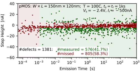
Fig. 1: The emission events from 65 pMOS transistors (W x L = 150 nm x 100 nm) have been extracted after each of the devices has been stressed for 1 ks at a gate stress bias of -2.4 V. The extracted emission times are observed to exhibit widely distributed charge emission times and step heights. With general-purpose instruments, almost 60% of the defects cannot be identified, as they would be obscured by measurement noise.
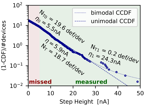
Fig. 2: Exponential distribution function of the step heights of the charge emission events from Fig. 1.
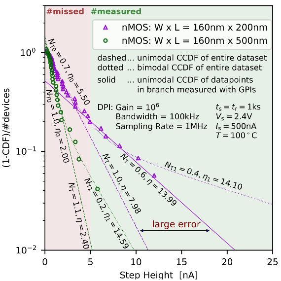
Fig. 3: The CCDFs of step heights of nMOS transistors exhibit an exponential behavior. In contrast to pMOS devices, the number of defects is significantly smaller in nMOS transistors, and thus, a high measurement resolution is even more important for accurate extraction of the CCDFs of step heights for these devices.