
 |
|
||||
BiographyBernhard Stampfer, born in 1989 in Austria, studied at the Technische Universität Wien where he received the Bachelor’s degree (BSc) in Electrical Engineering (2013), the Diplomingenieur degree (Dipl.-Ing., MSc equivalent) in Microelectronics and Photonics (2016) and the Doctoral degree (Dr.techn., PhD equivalent) in 2020. Bernhard is employed at the Institute for Microelectronics as a post-doctoral researcher and his work is focused on the characterization of defects in semiconductor devices. |
|||||
Statistical Characterization of Defects Causing Random Telegraph Noise
Random telegraph noise (RTN) and the related bias temperature instabilities (BTI) are two important reliability and performance concerns affecting modern MOSFET technologies. Both effects are caused by electrically active defects located in the insulating oxide of the transistor or at the interface between the oxide and the semiconductor. By measuring the drain-source current through the device and subsequently analyzing the recorded signals, information about the contributing defects can be obtained. This data can then be used together with charge-trapping models and device models to predict the reliability and degradation of these devices under various operating conditions (i.e. applied biases and operating temperatures). However, such characterization studies are complicated by the fact that modern MOSFETs contain only few of these defects, and the performance between individual devices varies.
By automating both the measurements and parameter extraction steps, a large number of measurements can be performed and analyzed, which allows one to efficiently extract the statistical distribution of various defect parameters. For this, we utilize RTN measurements, which are recorded using our semi-automatic probe station in combination with our in-house measurement systems. Afterward, the data is analyzed using an edge detection algorithm (e.g. the Canny algorithm) in conjunction with further processing steps for the extracted data. By doing so, the distribution of the defects' impacts on the threshold voltage, their capture and emission times at different gate biases and temperatures, and finally also the distributions of their depth in the device and their trap levels can be estimated.
In Fig. 1, a typical distribution of step heights extracted from Si/SiO2 devices is shown. Interestingly, the distribution seems to be bi-modal, with two underlying exponential distributions, indicating two separate defect contributions. Fig. 2 shows the corresponding distribution of trap levels obtained for these defects, which can be compared to results from atomistic simulations to learn about the physical nature of the defects.
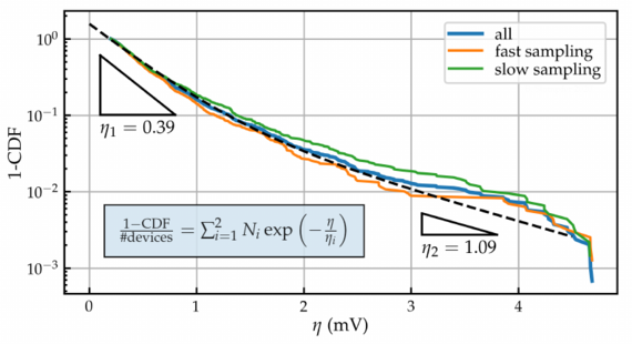
Fig. 1: Complementary cumulative density function (CCDF or 1-CDF) of the impact of the defects on the threshold voltage shift. As can be seen, the CCDF consists of two exponential distributions.
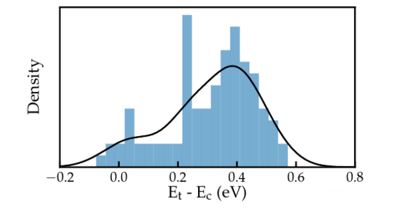
Fig. 2: Distribution of the extracted trap levels of the defects. The distribution shows its maximum at approximately 400 mV above the Si conduction band edge.